Introduction
In the receiver portion of my “25 Mbps discrete logic transceiver” project, I will eventually need a functional phase-locked loop (PLL) for one reason or another, but certainly for the clock data recovery circuit (CDR). Browsing the suitable components, that is, 5V CMOS, able to work with 25 MHz, not being super clunky and not needing an FPGA-level of configuration, I realized my options are quite limited. Actually, I don’t have many more choices than the chips based on the 4046 series.
The 4046 is an ancient chip with an integrated VCO and a couple of phase detectors. According to the datasheet, and application notes, it could be usable at 25 MHz, but the Internet is very skeptical about that. Apparently this chip doesn’t perform well at frequencies beyond a couple of MHz, it requires a cumbersome filter tuning and behaves very unreliably, depending on temperature, supply and configuration. People over at TI E2E forums are frustrated by the lack of documentation on working examples and configuration guidelines. There has been an intense discussion over at EEVBlog’s forum about it, as well.
Well, knowing all that, I decided to give this little guy a chance. This is a learning project after all, and learning how to make it work, or fail at it, is probably a valuable lesson.
4046 inside and outside
Phase locked loops work like this: there is a voltage controlled oscillator that changes its frequency depending on the small DC signal feeding it. There is a phase comparator that compares that VCO’s output with the input signal we want to get locked with. The phase comparator’s output is a signal proportional to the phase difference between VCO and the input signal. When all is good, and the PLL is locked, it should be zero. And lastly, there is a loop filter, that filters the phase comparator’s AC component and delivers the DC signal that controls the VCO. That’s it, a loop closed by the delicate balance of all the mentioned parts.
CD4046 is one of the oldest and simplest ICs that integrate most of the PLL parts into the single chip. Only the loop filter should be added externally, and a simple RC network should suffice. Of course, finding the proper R and C is where the true skill hides. Inner logic of 4046 is rather simple and self explanatory. There is a VCO, controlled by two inputs, VCO_IN and R2. The former one is a DC signal that, ideally, comes from the loop filter and tunes the VCO to the proper phase. The second one, R2, is a placeholder for a resistor that sets the offset voltage, in case we need an offset VCO frequency. There is also a capacitor C1 provided externally, which is used as the part of the charge pump – an oscillating circuit which actually creates the output oscillation. 4046 offers three different phase comparators, each with different phase-to-voltage transfer functions.

Setting up the VCO

As I mentioned earlier, the VCO works as the charge pump: the capacitor C1 is charged through the H-bridge G1 and G2. When the charging current is constant, and it is, the voltage across the C1 ramps up. When the ramp hits the FF threshold, H-bridge control signal reverses and the capacitor switches its poles, discharges through the diodes D1 or D2 and ramps up again, in a different polarity now. The FF output oscillates with period equal to the two charging cycles. The constant current that charges the C1 is controlled by the input VCO_IN and offset VREF. We can fix this value by choosing appropriate resistors R1 and R2. All of this is well described in the TI’s application notes, so I won’t go much into the detail.
What I want to get more detail into is the factors determining the output frequency. The application note above contains a straight forward calculation, but at 25 MHz things get a little bit tricky, as the various parasitic elements come at play. The FF propagation delay, parasitic capacitance and NMOS on-resistance become comparable to the external components we need in our configuration and cant get ignored anymore. So, let’s break it down.
The charging time of the capacitor Tc, when the current source is constant is given by rather simple formula
Tc = C Vc / IAlthough simple expression, there are some caveats. The first one is the capacitance C, which is of course our C1 but with the added stray capacitance Cs, in and out of the chip. The Cs is estimated around 6 pF in the app note.
The voltage Vc at the capacitor is the peak ramp voltage when the ramp hits the FF threshold. But there are two things to note here. The first one is when the H-bridge changes its drive, the previously positively charged side of the capacitor ends up at the lower potential of the H-bridge. Since the body diode is now forward biased to the GND, the actual voltage at this side of the cap is -0.7V. The total ramp is now upper threshold plus 0.7V. The second thing, during the charging phase, the current flows through the H-bridge MOSFETs which have a non-zero on-resistance Ron. Knowing this, the total voltage across the capacitor is reduced by the voltage drop on this resistance, that is, Vramp – I x Ron. The app note says nothing about Ron value, but the BASIC code in the Appendix C specifies this Ron to 50 Ohm, which is unusually high for a modern MOSFET.
And lastly, the current I is the sum of two current mirror amplifier’s outputs, defined as
Isum = M1 x I1 + M2 xI2where I1 is the modulating current set by R1 resistor, ( VCO_IN/R1), and I2 is the offset current set by resistor R2, (VCC – 0.6 V)/R2. M1 and M2 are two current gain factors, ranging between 6x and 8x but heavily dependent on VCC and bias currents I1 and I2. The best way to estimate M1 and M2 is to either extrapolate from the available graphs in the app note, or diving into the BASIC code in the Appendix C. There we have some expressions like M1=–.04343*LOG(I1/.001)+6 or M2=–.087*LOG(I2)+4.6+.4Vcc, which were obtained by someone in TI lab doing the fitting work ages ago.
Okay, I’m almost at the end, hold on. The output frequency is, as always 1/output period. Output period consists of two charging cycles, that is 2x Tc, and a time needed for the capacitor hitting the FF threshold and signal appearing the at FF output. This is propagation delay or Tpd, which is again VCC dependent and can range between 10 and 14 ns. In the BASIC code Tpd is estimated as Tpd = EXP (–.434*LOG(Vcc)–17.5).
Finally, the output frequency is
Fc = 0.5 / (Tc + Tpd)The ideal and clean design process would start by defining frequency range and the supply voltage, and it would end with required values for R1, R2 and C1. It would be an iterative work with many unknowns and heavily leaned on the empirical fitting from the graphs in the app note. It would also differ from manufacturer to manufacturer, if not even from batch to batch. For this reason, the purely analytical design process is not recommended.
What is recommended though is getting to know your VCO empirically. For this reason, I have developed a testboard with basic 4046 configuration and tried out to play with it until I understand how the VCO, and PLL in general behave.
Measuring the VCO
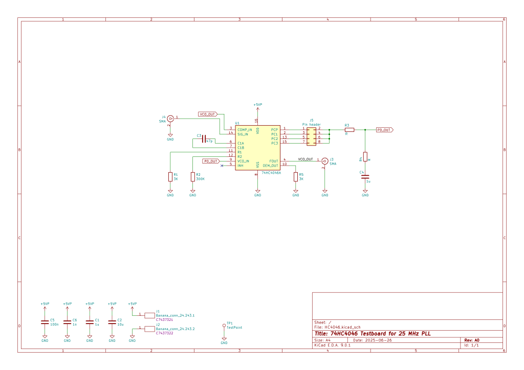
The schematic is pretty basic. I added some jumpers to try various phase comparators and SMA connectors for input and output signals. I attached the potentiometer at the PD_OUT connector, and observed how the frequency varies with various VCO_IN voltages. I changed the VCC from 5 to 7V and C1 from 15 fo 55 pF. I decided to go with Nexperia’s 74HC4046A, as it was readily available on LCSC, so some differences from TI’s specifications are to be expected.

I managed to reach nice and stable 25 MHz, which was a success on its own, given how the resources are full of skepticism at such high frequencies. The trick was to push the supply a bit above the max recommended 6V. The VCO got there using 3K for R1, 15K for R1 and 40 pF for C1. Then, I needed to test for the linearity and frequency span. I varied the VCO_IN using the potentiometer and got the following graphs.


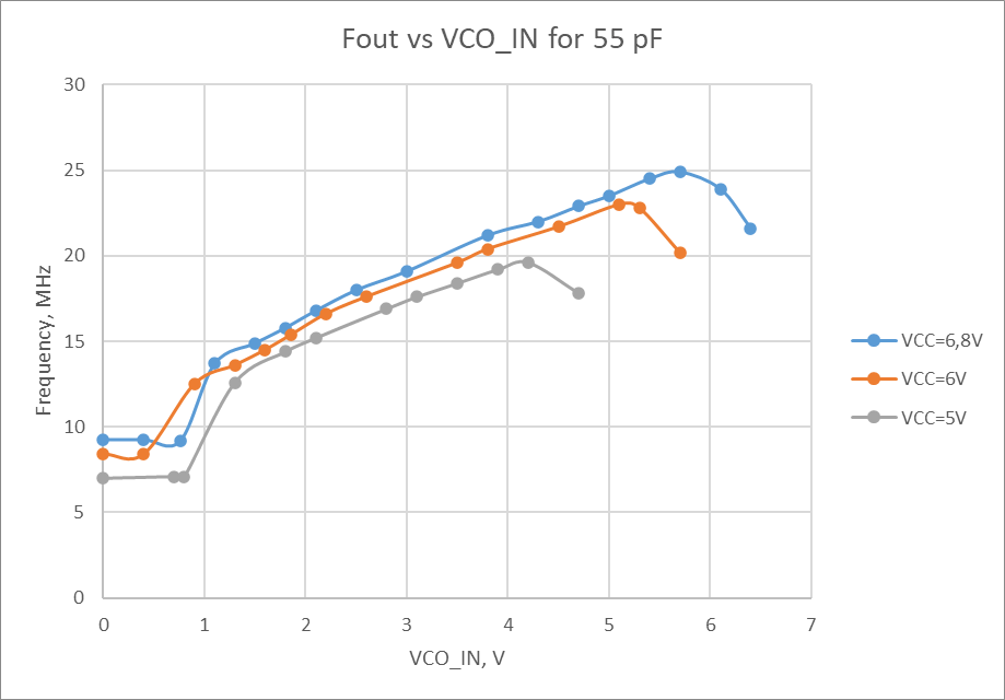
When C1 is 40 pF, we see a nice linearity but at relatively modest range, from 15 to 26 MHz. This was all at 6.8V supply. Lower voltages couldn’t reach the desired 25 MHz. This is much different then what can be found in the datasheet (Figure 19, where the same values for R1 and C1 are taken). My setup definitely couldn’t reach the 30 MHz, and it makes me curious how they got such a nice linearity in that area.
Reducing the C1 helps with higher frequencies, but linearity is poor. Increasing the C1 improves the linearity, as expected, but then VCO is unable to reach the wanted 25 MHz, which ends us in the non-linear portion of the graph. All that being said, I decided to settle with 40 pF for C1.

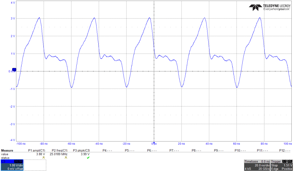
Below is the screenshot of the C1 charging waveform. There we clearly see the ramp during the half-period charge-up, followed by the flat voltage across the nMOSFET’s Ron resistance. We see how the charging begins at -1V, as the capacitor is being discharged through the body diode. The ramp ends up at cca 3V, what is the Flip-Flop’s upper threshold at 6.8V. Interestingly, TI’s app note specifies this value to be 0.1xVCC+0.6V, which ought to be 1.28V. Nexperia HC4046’s charging voltage is double that one of TI!
Phase comparators
VCO_OUT is compared to the input signal using three different phase comparators. There is a detailed description of each of them available in the device’s datasheet as well as in the app note, so I’ll just list the basic properties:
- The phase comparators generate pulse when signals’ phases are misaligned
- The average value of the pulse stream is proportional to the error signal, that, is the phase difference
- The average value is extracted from the loop filter while the pulse ripple is filtered out
- Each phase comparator has its own transfer function Kp, related to the phase difference, that is, PC average output vale. These are VCC/π, VCC/4π, and VCC/2π, for PC1, PC2, and PC2, respectively.
- Each phase comparator has the range it can detect phase differences in. These are 0-π, -2π-2π, and 0-2π, for PC1, PC2, and PC3, respectively.
There are some specifics to each phase comparator, selection of which is application dependent. In my case, I think I’ll opt out of PC1 as it has quite limited phase range, and it also specifies the duty cycle requirement to be 50%. I have a gut feeling it wont be suitable in my case. Let’s try with PC2 as it seems the most muscular one, with the largest working range.
Magic of the PLL
Configuring the VCO is a feat on its own, but the real challenge lies in making the PLL run by itself. The workings of PLL is well understood, and there are many resources on control theory of PLL, but each time we have new set of parameters, the PLL design gets monstrously more complex.
Let’s start with small steps. The transfer function of the VCO, Kv, in the linear area is extrapolated from my measurements and it is approximately 2.25 MHz/V. The transfer function of phase detector PC2, Kp is already said to be VCC/4π rad/V, or in my case 1.7/π rad/V. The open loop gain, that is Kv x Kp is then 2π 2.25e6 rad/s/V * 1.7/π V/rad = 7.65e6 s-1.
The loop filter, which defines the dynamics of the PLL, is the first-order RC network, defined by R3, R4 and C4 in my schematics. The transfer function of this filter is
Kf = (1 + sT2) / [1 + (T1 + T2)s] where time constants T1 and T2 are defined as R3C4 and R4C4, respectively. Together with the product Kv x Kp, the loop fiter forms the closed-loop expression which is a standard 2nd order system transfer function. Without going into the sausage long formal expression (which are available in any electronics circuit introduction textbook, as well as easily analytically deduced by oneself), let’s just extract the crucial parameters, that is the natural frequency ωn of the open loop, and its damping factor ζ.
ωn = sqrt [ Kv x Kp / (T1 + T2) ]
ζ = ωn/2 x [ T2 + 1 / (Kv x Kp) ] ≈ ωnT2 /2, in case of very high Kv x Kp like ours
At this point, we need to pick what we base our design on – is it settling time, jitter, noise or something else. If, for example, I want to synthesize a stable and clean clock, I would want to go for a low loop bandwidth and high damping. This way, the loop would filter out most of the noise what would result in lower output jitter and a bit longer settling time.
As you know, in my application this PLL is used for clock-data recovery on the receiver side. This means that PLL will deal with very noisy and unpredictable input signals, and should respond relatively quickly, It should be able to track the really fast changes, which requires a faster loop dynamics and wide loop bandwidth. This is very different requirement than designing the PLL for a low jitter clock source, where the lower bandwidth and longer lock-in times are needed. Loop bandwidth must be wide enough to track jitter on long PRBS sequences, but narrow enough to suppress high-frequency noise.
A good starting point would be 1 to 5% of the output VCO frequency, and damping factor of 0.707 (critical damping). In my case that would mean a -3dB bandwidth of up to 0.25 MHz. From the 2nd order system analysis, natural frequency can be found as as
ωn = 2pi fBW / sqrt ( 1 + 2ζ2 ) = 2pi 1.25e6/sqrt(1.5) ≈ 2pi 180x103 rad/sMeaning that natural frequency is at 180 kHz. This is where the 2nd order system resonance peak is. The time constants sum is then
T1 + T2 = Kv x Kp / ωn2 = 7.65e6 / 1.27e12 = 6.2 μs
Knowing damping factor ζ=0.707, we can figure out T2 to be 1.1 μs. This makes T1 to be 5.1 μs. If I use the standard 10 nF for C4, the R3 must be 510 Ω, and R4 must be 120 Ω, to get to the approximate values.
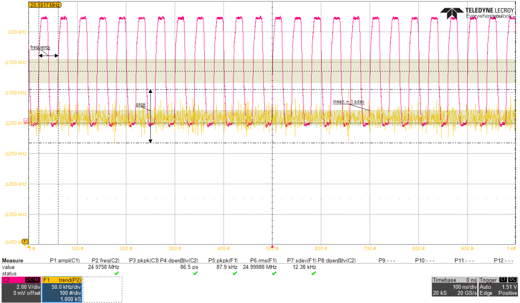
I attached the signal generator, and tried varying the output frequency. The PLL managed to lock relatively quickly, and the output frequency was stable. The input signal from my Agilent signal source, shown in yellow in the video capture below, should be a nice square signal, but it obviously isn’t. The reason the input signal is so bumpy is of course the impedance mismatch – the signal is T-split at the source, where one end goes to the scope input, terminated with 50 Ohm, while the other ends up in the 4046 input, terminated with 150 kOhm, that is effectively, open end. This makes the stub out of coax cable and causes the reflections at the scope that we see as the bumps. The VCO output signal is shown in magenta, and it resembles a proper squarewave, as its line is properly terminated. Blue waveform shows the lock signal, that is the PCP_OUT, active high when the loop is locked. You can see how the PLL stays locked up until 27 MHz, when it suddenly starts jumping around, before it returns to the stable range.
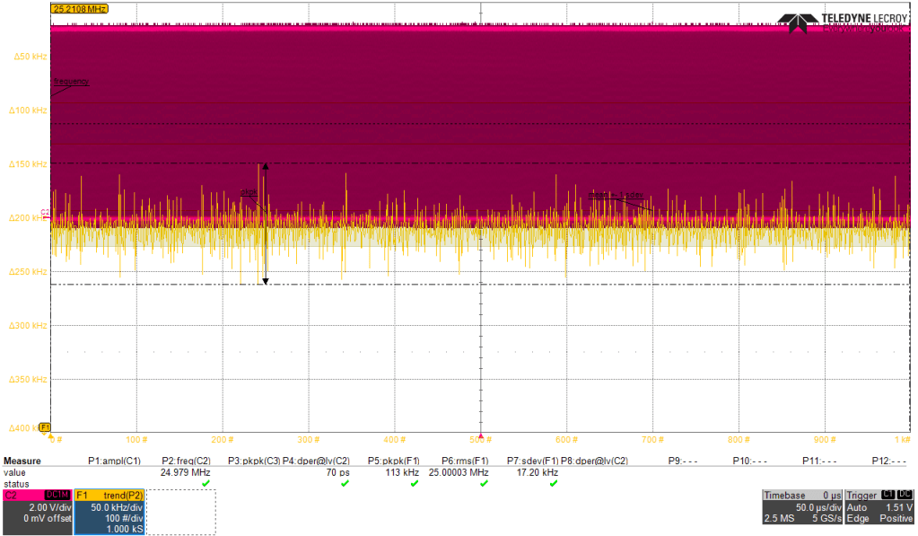
Here is some frequency stability analysis I did over the various time durations. During the 1 us, there was standard deviation of 12.4 kHz with peak 44 kHz deviation. During the 50 us, there was deviation of 17.2 kHz with peak 56 kHz deviation. During the 2 ms, there was deviation of 67.7 kHz with peak 211 kHz deviation

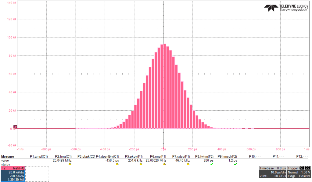
Usually, for jitter measurements are better suited histogram distributions. Below we can see that median jitter of my Agilent signal source is 1.2 ps with FWHM spread of 280 ps. The locked 4046 has median jitter of only 7 fs (!) with the spread of 101 ps. Does this suggest a hard-to-believe fact that my pretty rudimental PLL has better performance at 25 MHz than the industry standard metrology equipment?

Okay, I guess I have a functional PLL for my 25 Mpbs transceiver. But will hold up to the challenge of clock-data recovery? Let’s find out in the coming weeks!
