Introduction
In my previous post, I talked about the design of a simple 25 Mbps transmitter with PRBS generator, encoding and pre-emphasis. I designed the circuit using the discrete logic components in order to get a better understanding of modern transceiver circuits. Since the standard (25 Gbps and higher) transceivers are implemented in the silicon of FPGA or ASIC, I had to get down to 25 Mbps in order to make it feasible in the human scale PCB technology.
Prototype bringup
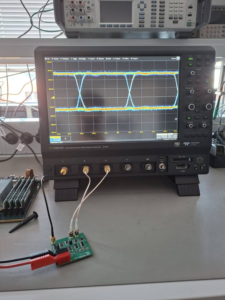
Few weeks later, I got my fully assembled prototypes. No soldering issues, no bad placement, clean silkscreen printing. JLC did a good job here. I connected 5V bench power supply and hooked up the coax cables to the 4 GHz oscilloscope, and happily established that nothing went broken, nor burned. To my delight, the PRBS generator seemed to work just fine, producing nice NRZ signal, spectrum of which corresponds to the expected one:
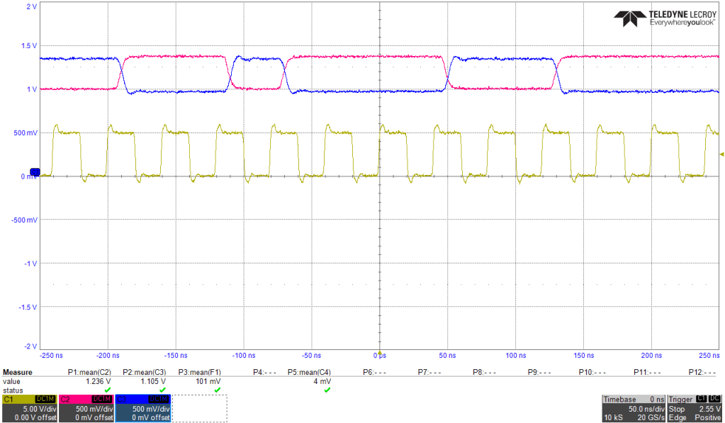

Line driver needed some tweaking. As I left my placeholder resistor R13 in the P-side follower to be 100 Ohm value, the total gain was 1.1x. At the same time N-side gain was 1x. This 10% gain difference cause a notable asymmetry in the waveforms on P and N outputs. Shorting the R13 solved this issue and ensured a nice and symmetric eye-diagram:

Pre-emphasis debugging
I was not so lucky with my pre-emphasis circuit, though. The circuit does its job well, be XOR-ing delayed signal with the original and summing up all the taps, but there was a certain timing issue. First, I noticed the pre-emphasis boosts at the wrong time – instead at the transitions, they appeared somewhere in the middle of the high level phase. Then I realized that my signal has double the delay time between tap 1 and the original. This felt really weird…

I got back to the 74AHC595’s datasheet, looking for what could be wrong, checking all the delay parameters, and everything seemed reasonable enough. Until I found that the 74AHC595 has actually two registers, one for shifting and another for storage. The taps (Q0 – Q7) are driven out from the storage register, and this one is always one clock cycle lagging, behind the actual shift register. That’s why my 1st tap is two cycles behind the original, but 2nd and 3rd are 1 cycle behind that one. Damn.

Luckily, this is easily fixed, thanks to me settling down for the SOIC package. What I need to do is to use Q0 output as my “original” signal for the pre-emphasis, and Q1 to Q3 as delay taps. I did some on-board re-wiring and managed to get my pre-emphasis in place.
Partially, at least.

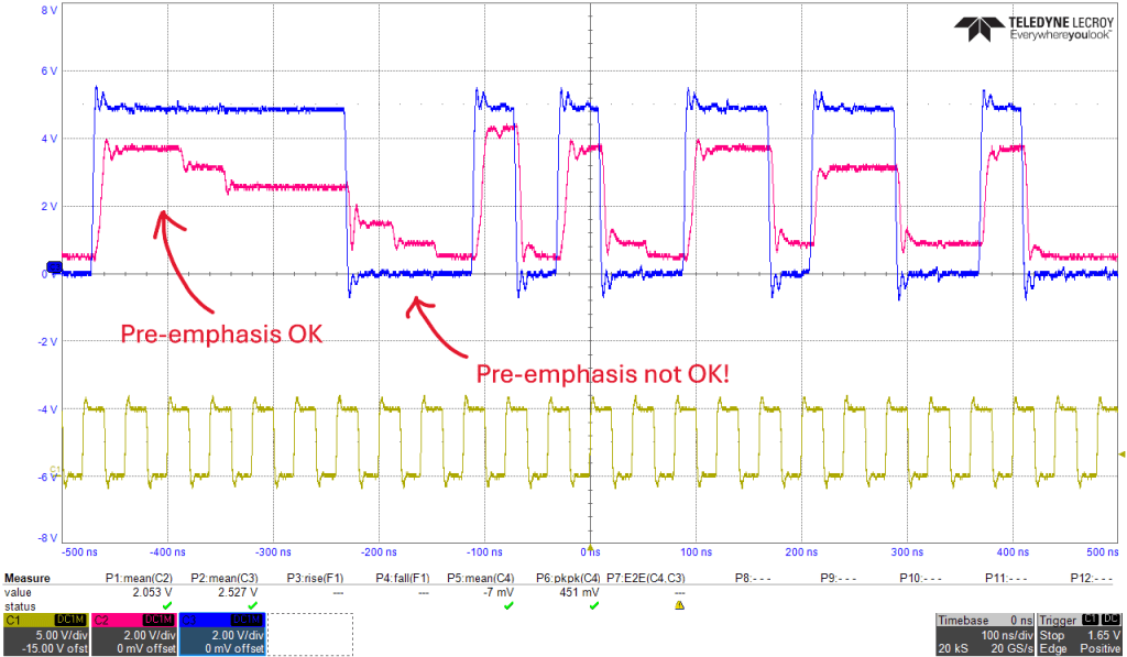
Because, the pre-emphasis didn’t work well in the high-to-low transition. Why is that so? Well, the reason is quite simple one, and if I paid a bit more attention to the circuit design earlier, it would be easy to detect it. The matter of fact is that XOR output contributes with some voltage when the signal and its delayed taps are on different levels. In case of low-to-high transition, this is desired so. But not so much in the case of high-to-low transition. The XOR will lift the signal off of 0V, creating the undesired, dampening effect. Damn, indeed.
How to fix it? Obviously, the pre-emphasis cricuit will need some re-designing. Off the top of my head, adding AND gate should at least differentiate between H2L and L2H transitions and keep only the L2H portion of the pre-emphasis. For the other case, I’m still looking. Most likely, I’ll need a different circuit for each case and sum them somehow up.
Encoding debugging
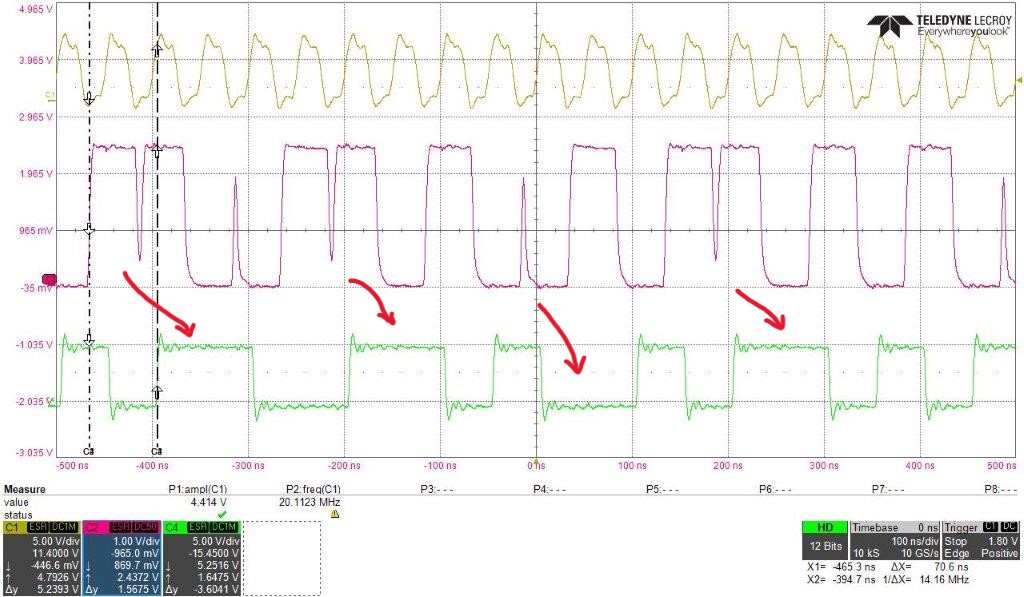
I wasn’t lucky neither with the Manchester encoding. The circuit worked as it should, creating the transitions instead of having flat lines, but there was something peculiar.
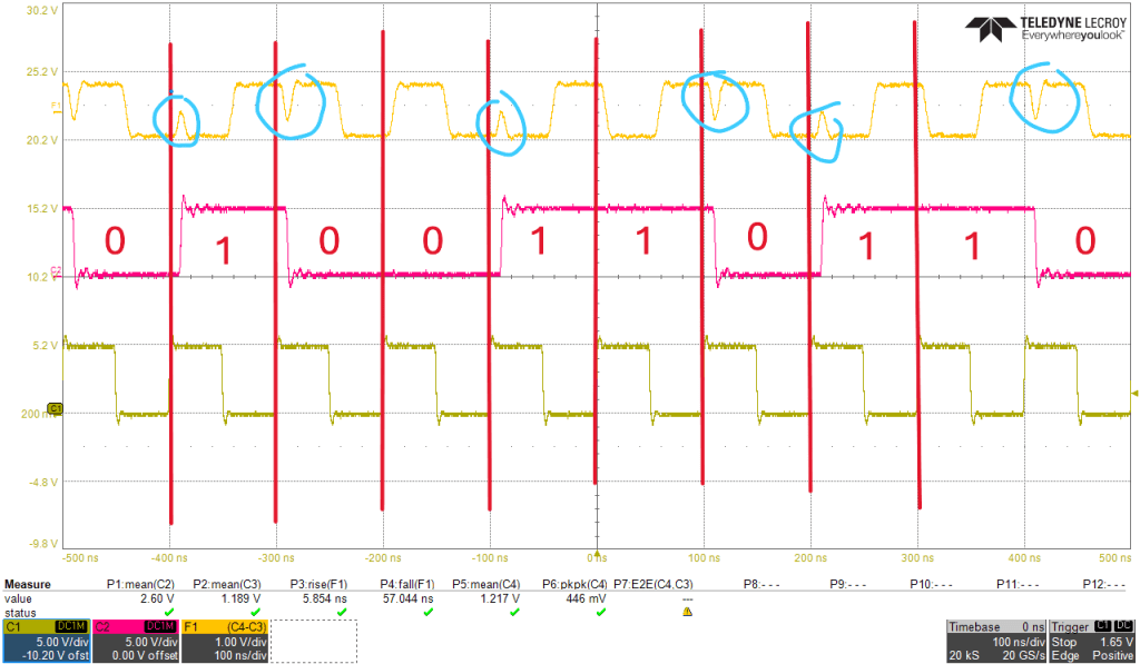
Manchester code works like this: when the incoming bit is 0, the encoded data looks like the clock cycle (first half is high, second half is low). When the incoming bit is 1, the encoded data is inversed clock (low-to high). The issue arises when signal and clock are not perfectly aligned. In my case, the signal lags 8 – 10 ns behind the clock, as is specified in the 74AHC595 datasheet. The XOR gate will keep on XOR-ing during this time and, if the data changes, it will result in a sudden glitch just before the encoded symbol starts.
This two images below depict that reasonably well:

What to think of it? Well, the glitch issue arises because the clock and data are not in perfect sync. How come, since they are synced the best they can be, as the data comes out of the clocked FF in last stage of the shift register 74AHC595? Well, the XOR gate pushes them a bit out of the sync and this ought to be corrected by adding another syncing circuit, that is another FF-gate just after the XOR gate. However, since the number of transitions has doubled, this clock should be at the doubled frequency, which in my new case is 20 MHz.

I modified my board a little bit – I’ve repurposed one 74AHC595 shift register from pre-emphasis circuit to the encoding improvement. Luckily, there is already data in and out properly connected, with output coming out at pin 15 (Q0). But two clock pins had to be lifted off the board and fed with external 20 MHz clock source.
To sum up, my next revision of the transmitter circuit will have to deal with two issues:
- Synchronous Manchester encoding. This implies adding an extra clock source, which is 50 MHz. This may require changes in my logic family choice, as the propagation delay required should be much less than 20 ns.
- Improved pre-emphasis. This will be done either on digital side, by adding the AND-gate to the existing circuit and making separate pre-emphasis for both positive and negative edges. But, as we learned from the encoding section, this will introduce some un-syncing, therefore, each AND-gate output should be synced again, by the extra FF-gates. The whole thing gets even more complicated knowing that doubled clock rate is needed in pre-emphasis circuit too, if the encoding is used. Maybe the analog side pre-emphasis at the LVDS driver might be a better option?
