Introduction
Last month I won a EuroDOTs scholarship to take a 2 – week training course called “Integrated magnetoresistive sensors: from material deposition to wafer level testing” at the Institute of Microsystems and Nanotechnologies (INESC-MN) in Lisbon, Portugal. Sounds quite badass, huh? Well, it is, cause the INESC truly is the best portugese research institution and enjoys the strong relationship with both industry and universities of Portugal. The aim of the course was to design and develop the magnetic thin-film sensor and their optimization for wafer level testing. I was hosted by prof. Susana Freitas and her team consisted of PhD students and post-docs: Diana Leitao, Jorge Amaral, Ana Silva, Joaó Valadeiro, to whom I am deeply grateful for all the time and effort put in my training and providing me the best possible insight in the subject.
So what was I doing there? Well, designing the magnetoresistive sensors. It’s all about some really super awesome sensors which can sense extremely low magnetic fields and you have been probably using one of them whenever you played with some kind of compass application on your smart phone. But actually, these are used for many other sensing purposes than just a smart phone apps. The physical principle behind their work is the change of electrical resistance caused by the present magnetic fields. So to put it very simple: you apply a constant voltage across the sensor and you measure the current which passes through. Depending on the magnetic field, the current will change and you can read out the field strength from it.
I shall divide the post in two parts, to make a better order of the text. First part comes directly in this post, and it will cover general overview of nanotechnology facilities and work in clean rooms, as experienced by myself during this course. Second part comes in a separate post (available here) and it will cover basic theoretical and practical aspects of magnetoresistance and magnetoresistive sensor design. It is not necessary to read the theory intro before to understand the first part, but it may be helpful for the better insight in whole developement process.
Clean room
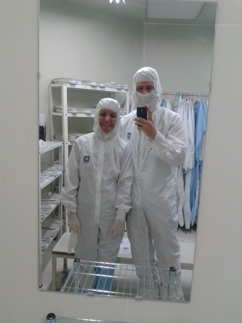
Laboratories where silicon chips and microsystems are produced are called very conspicuously the clean rooms. As the name suggests, they are very clean. But did you know there is a measure of cleanliness? ISO 14644-1 is a clean room standard and it defines few classes of cleanliness. In example, at INESC there are rooms of class 10, what means there are no more than 10 000 particles bigger than 0.1 μm within one cubic meter. Also, there are no more than 1 020 particles bigger than 0.3 μm, and no more than 83 particles bigger than 1 μm within the same volume. This is very, very clean. And to keep it that way everyone who works inside should wear the special suit like I did on the photo here. Contrary to what it may look like, the suit is very comfortable and protects me from both chemicals and electrostatic discharges (yes, it is interlaced with tiny metal fibers to spread out evil charges). But it is not so much about protecting myself as protecting the clean room from me: our body is covered with stuff which should in no conditions whatsoever contaminate the clean room.
Once the suit is on, we can enter the clean room. Inside, there is all this super-fancy equipment used in nanotechnology:
- ion-beam deposition machines,
- ion-beam etching machines,
- plasma sputtering machines,
- photolithography machines,
- electronlithography,
- resist dispensers,
- resist developers.
- laser exposition devices
and lots and lots of other chemistry playthings. I’ll try to get them all covered in this post.
Fabricating the sensor
Wafers

It all begins with the silicon wafer. This is nothing more than a thin slice of silicon crystal with very high purity (more than 99.999 %). They are usually made in disk shapes of 6″, 8″ or 12″ in diameter, few hundreds of μm thick. Everything we do from now on is on this wafer – film deposition, lithography, etching, printing etc. In the end, we shall have a silicone disk covered with (up to thousands of) various structures with varius film layers. Each of the structures is called a die and this is what is finally cut out of silicon wafer and embedded in our microchip.
This is the basic of almost all of the nano- and microtechnology – this is the way all integrated circuits are made. Not only magnetoresistive sensors, but also all of the modern semiconductor electronics, starting from basic transistors to highly integrated microprocessors in your PC or cellphone. If you like to play with the electronics, and you buy some general purpose chip, say amplifier in DIL or SMD package, and if you slice it and look under the microscope, what you’ll see is very small die on the silicon wafer with many layers of different materials and interconnections.
Thin-film deposition
This is not a “camera” kind of film, to make it clear immediately. Many people get confused at this point when we talk about this. Thin film is just a layer of material not more than few micrometers thick. Actually, it is usually few hundreds of nanometers thick. People often do not have perception of how thin this is. Take your desk ruler and find a millimeter on it. Now imagine, what is so small that fits 10 times within? Well, normal paper is, and it is 100 μm thick. And now imagine, what is so small that it can fit 100 times in one millimeter? Human hair! 1000 times? Very small cells and bacteriae! 10 000 times? Viruses … and thin films. Yes, this is the size of what we are playing with here. But it does not end there – we are able to play with even smaller sizes in this kind of the laboratories: deposit films of few angstrom. 1 angstrom (Å) is 10^-10 m and it is approximately size of phosphor, sulphur or chlorine atom. In other words we, are able to manipulate columns of only ten atoms! I find it extremely amazing. It is all thin-films! Think about it next time when you find it impossible to slice your onion thin enough.

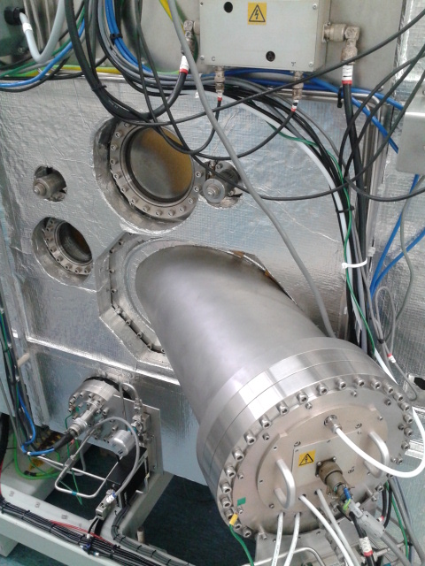
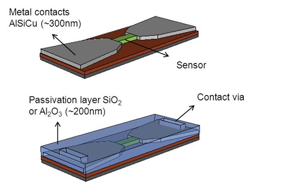
Now back to the sensors. One typical spin-valve magnetoresistive sensor is made up of 7 thin-film layers (picture on the right). So, the first step after taking an empty silicon wafer is to cover it with the few nanometers thin layers of copper, tantalum, cobalt-iron alloy etc. But how to do it? You can’t just spread on layer of ten copper atoms on the wafer like you would spread Nutella on slice of bread! In “normal” technologies, people use electroplating – but that involves electrodes in situ and you couldn’t make layer fine enough. In nanotechnology, we fancy many different methods to create such stacks. At INESC-MN, I worked with ion-beam deposition (Nordiko 3600 Ion Beam) and I’ll try to briefly explain how it works.

So, you start by gentle cleaning your silicone wafer and placing it in the deposition chamber. On the right photo, a colleague puts his wafers on the substrate holder which is later to be placed in the ion-beam deposition machine, standing just behind him. How does this machine work, you ask? Well, here it goes.
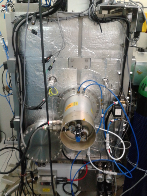
First, everything must be in the insanely extreme vacuum (10^13 times lower than the atmosphere pressure), which is obtained with turbomolecular and cryogenic pumps. Inside the chamber, you have an ion gun, shooting xenon ions with the energy of few keV to the something we call “target“. The target is basically just a brick of material we want to deposit on the wafer, such as CoFe or Cu. The Xe ions bomb the particles of the material off the target and these are kicked onto the silicon wafer. The ions are accelerated, focused or deflected using strong electric or magnetic fields. With the controlled and time-consuming process, particles are deposited in very fine layers. Depending on atomic energy and surface tension, particles will spread uniformly or cluster in one place. Allowed roughness is less than 2 atomic layers, and adhesion, surface waviness and grain size are measures of deposition quality.

After cca. 3 hours long process is over, we have a silicon wafer covered with few layers of thin-film. With our naked eyes we can not see much, cause it is just a metallic reflective surface, so we reach the help of microscope to inspect the quality of the deposition.
Photolithography and etching
The point is not to have whole wafer surface covered with thin-film layers. The point is to have only small structures, in size of few micrometers (remember, we are working with microsystems) placed at some specific points on wafer. That’s why we will etch the substrate – remove all the thin-film layers except on tiny places where we need them. Such a waste of good thin-film, you might think. But that’s how it is, life is hard in nanotechnology world.
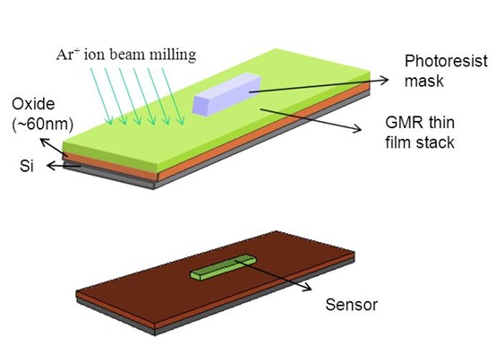
First thing was to apply the photoresist. This is a kind of substance that will be destroyed when UV light shines on it. Oh, yeah, there is also a negative photoresist which will be hardened once the UV light falls on it, but we won’t use it here.
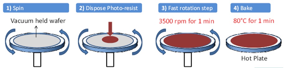
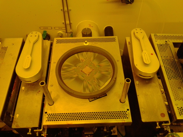
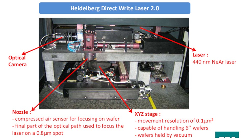
So, we take the wafer, place it on the coating machine and drop a droplet of photoresist on it. The machine will spin the wafer to 3500 rpm and centrifugal force will spread the resist uniformly all over the wafer. Wait some time for the resist to stiffen at the 80°C. The photo below which shows the coated sample is a bit yellowish because the room is illuminated by UV-free light source. Once the wafer is coated, we use laser to illuminate parts of the resist that we want to remove. How the laser knows which parts to illuminate and which not? We control it with computer program and the program reads CAD file that we have prepared before. This process, called photolithography, is more often done with the UV lamp and photo mask, but masks for such small and sensitive structures are enormously expensive, especially for the research samples where the layout is constantly changing. After laser exposition, the film is developed – which means it is washed in some basic or even acidic solution to remove the parts of the resist “destroyed” by the laser. Developement process is performed in similar manner as deposition: you make everything spin at the high rate, drop a bit of developer solution and wait some time for reaction to complete, all at the cca 113°C.
Now follows the etching. For that, we use the same Nordico machine as for ion-beam deposition, only this time we use only assist gun – a beam of argon ions that shoots directly to the sample (so no targets this time). The process is called ion-beam milling. Accelerated argon ions will kick out all the parts of substrate that are not protected by the photoresist, and in the end we well stay only with the silicon wafer and tiny thin-film structures on the wafer. Why not use classic wet-etch, where we just immerse our sample in, say, copper chloride with peroxide? Because, here we have extremely tiny structures where chemicals could easily destroy from side. If we use ion-beam milling, we ensure high-definition of etch process and good preservation of structures.
All remaining resist is removed in the ultrasonic bath. Quality of the etching process may be observed under the profilometer – highly precise device that sweeps tiny needle across the surface of the wafer. Altitude of the needle gives us an estimation of surface roughness. An alternative is to use the reflectometer – beam of light being reflected from the surface will be at the different angle for various surface heights.

Metallization
Ok, we have silicon wafer and tiny thin-film structures left on the desired places on the wafer. Now what? We have to access this structure somehow. That’s why we shall deposit some conductive pieces on the wafer. Copper, gold, or silver can be used, but we used aluminium.

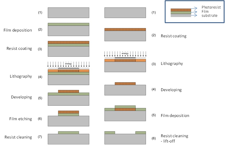
To do that we go again to photolithography room, coat the whole wafer in the photo resist, expose it in laser, and develop. But this time, CAD file contains layout of conductors. Note, our substrate now has resist there where aluminium leads should NOT be. Why is that so? Because now, we won’t use the etching process but something called a lift-off process.
Plasma sputtering was used to deposit 3000 Å thin film of aluminium all over the wafer. Did you get the picture? We have silicon wafer, few groups of magnetoresitive stacks, photoresist everywhere above except where the connection leads should be, and now all of that is covered in very thin aluminium. At the first, it doesn’t seem to make sense, but on the second – the sample is immersed in the solution which will dissolve all of the photoresist. The aluminium which covered the resist now has no ground to stick on and it will be disposed from the wafer. But the aluminium that was not spread over the resist will firmly stick to the wafer and remain intact. This is how we’ve created the aluminium leads for the magnetoresistive sensor, which can be now accessed from the outside. What people usually do, but I didn’t, is passivation – applying layer of insulator (usually some silicon or aluminium oxide) to protect the structures from oxidation or other evils of external world.
Packaging and characterization

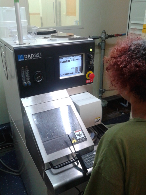
Once we are more or less sure that wafer looks good, we may want to put it in something more comfortable. The suits for sensor will be standard DIL package, where we will use golden wire bonding to connect sensor aluminum contacts with casing pins. But remember, on the wafer we don’t have just one sensor – we have maybe hundreds. To cut them out, we’ll use sophisticated method of cutting called dicing. It is nothing more than using very precise automated diamond saw to cut small pieces of wafer. And this small piece, if you recall, we call a die. The die is then placed in plastic package and bonded with 100 μm thin golden wire to it. Now we can use it as any other electronics IC!
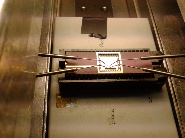
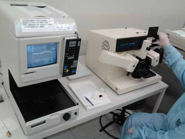
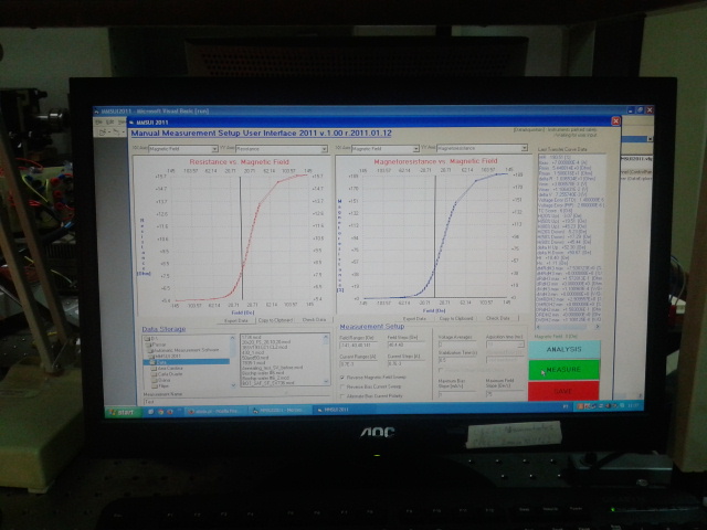
Here we see a typical 4-probe test set-up. The sensor is placed inside the alternating homogeneous magnetic field (within a Helmholtz coil). Voltage of 5 mV is applied on the sample and resistance is calculated automatically, by help of the computer program. In the end, we get a nice transfer function which describes dependence of the electrical resistance on the magnetic field, which is the main characteristic of the magnetoresistive sensor. Nominal value of the resistor was around 65 Ω, with magnetoresistance ratio of 6% and linear range from -20 to 0 Oersted. More details about how the sensor works and physical principles of magnetoresistance I’ll try to cover in the next post.

You explain this very well. Technical but easy to read.