Introduction
Working in a microwave engineering area I learned that classic components like capacitors or inductors are ditched away from the filter design and so called distributed elements are used. It means, basically, that inductances, capacitors, LC circuits are created using conductive lines on PCB instead of soldering old school components. Pretty cool, I thought, let’s give it a try…
A bit of cool theory of distributed elements
You can intiuitively guess that a long line connected to the GND will behave like an inductor. There is current flowing through it, there is some magnetic field, so it does reminiscent a coil in some way. In a similar fassion you can imagine that long track left un-connected will behave as a capacitor: no current flowing at the end of it, and some electrical field is forming. Actually, transmission line theory gives you an exact formula for impendace of this kind of lines: 


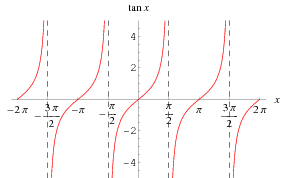
Funny thing with those tangent and cotangent functions is their discontinuity. For certain values of 

Why is all this useful? For one, it’s cheap and you don’t need to buy nor solder components. Second, at microwave frequencies, it is close to impossible to find proper component values for certain application. Designing filter, your calculation will tell you that you need some inductors in range of picohenry or capacitors in femtofarad. These atrocities are either extremely expensive or even unfabricable.
Filter design or bunch of math that you’ll definitely get wrong
To understand how to use this fantastic feature of TX lines for a filter design, you need a lot of tedious math and old fashion hand calculation. Pozar’s famous Microwave Engineering is a good start – you’ll learn which components you need for your filter and using Richard transformations and Kuroda identities convert those value to the line parameters. Than you’ll do a lot of calculation, fill in multiple sheets of paper with formulae and numbers and then throw it all in garbage.
Don’t get me wrong, I’m not saying anything against analytical approach but error prone humans like myself end up in a frustration alley after multiple attempts of “new sheet, new calculation, this time I won’t make a mistake”.
Anyways, back to design. Check the textbook, Chapter 8 on filter design and get it started. Fast forward approach:
- Define your center frequency and bandwidth (for me it was 1 GHz and 0.15 relative bandwidth)
- Choose filter order and type (I picked equal-ripple n=1 cause I didn’t want to bother too much)
- Pick a desired ripple in the pass band
- Get the g-parameters from the table (some smart people made tables for filter design that work. Why not use them?)
- Freak out cause those tables are for low-pass filters only!!!
- Relax and realize that it is supposed to be transformed to band-pass using frequency substitution, uh…
- Choose the topology to your own taste and …
OK, no rush here. Microwave filters are no joke, as every piece of copper on your board does something. To realize filter with distributed parameters there are multiple topologies: either using stubs and TX line sections, stepped impedance filters, coupled line filters or resonators. More details are, of course, in any book on microwaves.

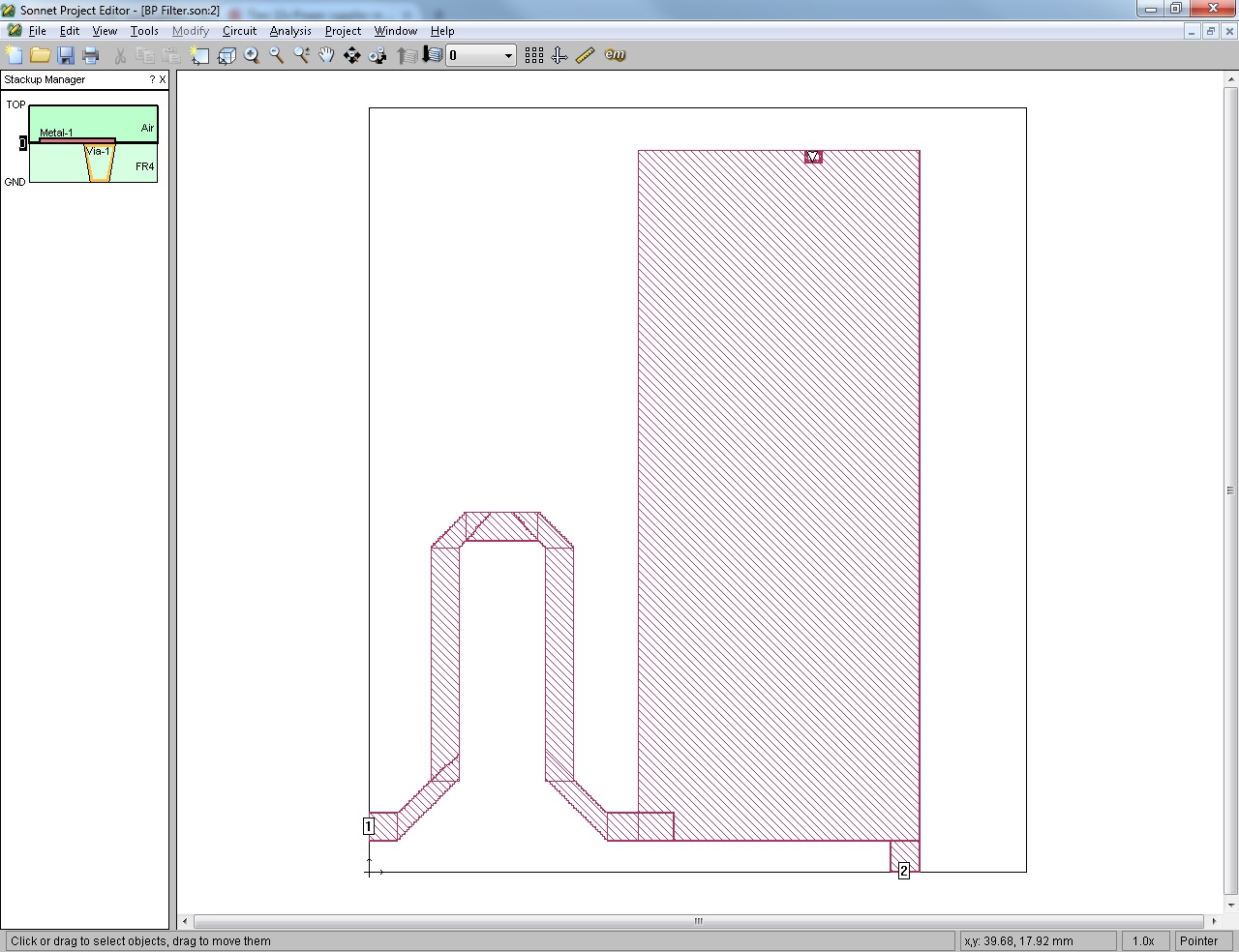
I decided to go for quarter-wave resonators as those are the simplest for me to comprehend. In lumped element form it looks like something like the image on the right. You can immediately see why is it band-pass: for low frequencies C1 is an high impendance element and L2 is short circuit, so output will be close to zero. For high frequencies L1 is super high impedance and C2 is short circuit so again the input will be cut off. Only somewhere in the middle, around resonant frequencies of L1 and C1, L2 and C2 we can expect some passage from the input to the output.
In my design L1-C1 and L2-C2 are both replaced with the quarter-wavelength long line and shorted stub, respectively. But what should be length and characteristic impedance of each? That strongly depends on how you chose your g-parameters and filter bandwidth, so get back to textbook, as there is a certain formula. For my purpose, 


Simulate and you’ll be wrong a little less
Working in microwave, you have to simulate everything. The analysis is often either to complicated and exhausting or over-simplified and won’t serve its purpose. That’s why there are many simulation toolboxes out there using finite element methods for you to finish your design with as little headache as possible. The most popular ones in RF and microwave design are CST and HFSS, a little less powerful AWR, sometimes even AnSys or Comsol Multiphysics. For this “simple” project of mine I decided to broaden my horizons and try out some less familiar but free solution. So I stumbled upon Sonnet Lite software, limited with crappy user interface and 32 MB of solution memory capacity. Anyways, an engineer is as good as much he can handle the limited resources so I decided to go for it. User’s manual by your side, you get standard procedure of 3D (rather 2.5D) simulation: draw geometry, define materials, define electrical ports, mesh, set solver and press “play”. I picked geometrical parameters (line width, length etc.) as was roughly estimated in the textbook, hoping that simulation will give me a chance to fit them later. Should I have played it well, pleasing solution should come out soon.

Simulation output is given as a distribution of electric and magnetic fields, but it’s not what I’m looking for. I’m interested in S-parameters, as they uncover the true nature of the filter: reflection and transmission coefficients.
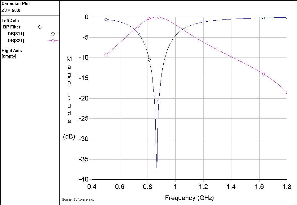
There we go. According to the simulation the output is not bad: center frequency is a bit off but return loss (reflection) in the pass band is less than -35 dB. Bandwidth is also a bit wide, but that’s expected from a 1st order filter.
Make the filter and see how wrong you were
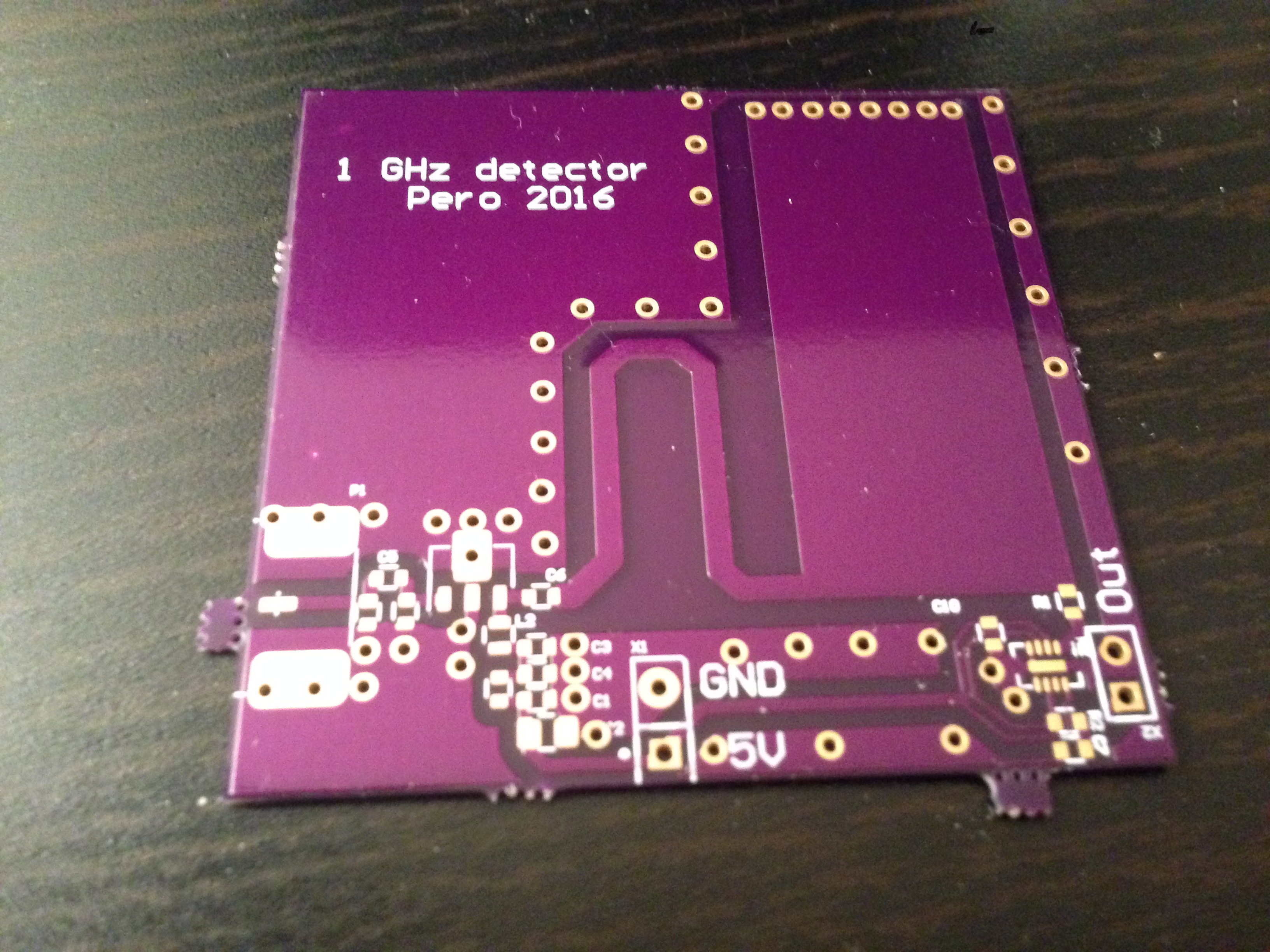
Filter was a part of my 1 GHz detector circuit board which I let OSH Park to fabricate. OSH Park is a friendly community of inexpensive PCB producers and they’ll cover your PCB in a nice purple solder mask. And the PCB will be nice in general.
At this point, I’m only interested in filter so I don’t solder any components. Instead, I scratch a bit of this beautiful purple solder mask and solder two semi-rigid coax cables, one at the filter input, other at the output. Then I plug them into my vector network analyzer and wait for the moment of truth.

Whoa! Center frequency is perfectly fit at 1 GHz! Is it possible that simulation got it wrong? Yes, it is, as simulation worked with pretty coarse elements which ruined the smoothness of geometry. However, you can see that simulation showed a bit more idealistic characteristics since the real return loss is not lower than -22 dB and insertion loss is a couple of dBs.
Not bad for the first try. Now, I have seen with my own eyes how nimble handling of simple copper traces can benefit your circuit design and show you wonders of microwaves.

Great blog I enjoyed readiing