Introduction
I am about to build a full PHY (physical, duh) layer for data transmission that simulates the multi-Gbps transceiver circuits usually seen in high-end FPGAs and ASICs. The reason I’m doing that is to get a closer understanding of the inner architecture of these advanced circuits, so ubiquitous in modern communication systems. To really gain that closer understanding, I want to do it using the discrete logic parts, like the old-school 74 logic family. Since the whole circuit is going to be rather big and clunky, I don’t expect it to work anywhere close to the Gbps range. But 25 Mbps might just be doable – we can simply pretend that we are looking at thousand-fold rates usually seen in 25 Gbps/28.3 Gbps systems. Also, 25 MHz gives just enough of high-frequency challenges to get PCB design a bit more interesting.
What I’m hoping to get from this?
I hope I’ll be able to understand how blocks in typical high-speed transmission work, such as pre-emphasis, de-emphasis, clock recovery, encoding, decoding, and similar. I hope I’ll be able to test them all on my lab bench, using the standard lab equipment. And to crown it all, I hope I’ll be able to get some nice eye diagram plots.
Part One – the transmitter
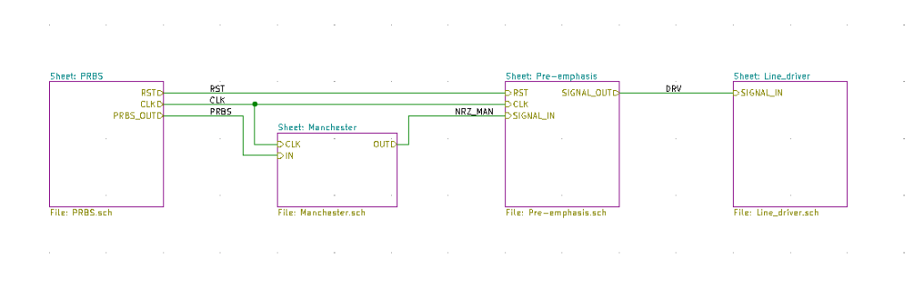
Making communication system only makes sense if there is a data stream ready to be sent. In my circuit board, I don’t want to bother with any large data files or some actual TCP/IP stream, I just want to push some random bits down the road… what did you say? Random? Well, hello, then the perfect source of the data would be a random bit sequence generator, or more officially know as a pseudo-random binary sequence (PRBS) generator. I intend to make this one using the linear feedback shift register 74AHC595 and I want to make it 2 billion-bit long. Luckily, I don’t need 2 billion ICs for that, 5 will do, since that is enough to build a PRBS31 generator. A bit more details on PRBS generation algorithms is available on this DigiKey blog post.
In communication systems, data traveling across any real channel, that is, a lossy channel, loses some of it’s signal power. The channel attenuation is stronger as frequency goes higher, so any nice square-shaped waveform get smeared and curvy. The engineering trick to fight this loss is to add a little bit more high-frequency content before the signal leaves the cozy harbor of the transmitter. This is called the pre-emphasis, and it makes square-shaped signal all spikey around the edges. The hope is, once the channel attenuation does its thing, and the signal arrives to the safety of the receiver, the spikes will be gone and the square-shaped waveform shall prevail. I plan to build the pre-emphasis filter using the 3-tap analog FIR filter. It sounds counter-intuitive (isn’t the FIR filter digital?), but in reality, all I need is a delay line and the analog summation. I will build this by using the 74AHC595 shift-register again and high bandwidth op amp summation circuit.
If somebody is ever going to receive this signal and verify that communication channel works, it should know the exact clock rate. But what if they don’t know it? Then, they will recover it from the data stream. See, there is a way to encode the clock information into the data, by using some form of the encoding. There are various ways to do that, but for my purpose and simplicity of the design the Manchester encoding is perfect.
Finally, the last part of the transmitter will be the muscle of the transmitter, that is the line driver. This is the piece of circuit that should conform the standard LVDS signaling and be able to push differential signal into the lossy 100-ohm differential line.
Transmitter Circuit Design
Aside of the mentioned frequency constraints, there are more practical ones, too: I don’t want to spend too much time and money on this. For that reason, I want to use ready available off-the shelf-components, I want to go down with component price as much as I can, and I want to let other people do the manufacturing job for me. For this reason, I intend to use the LSCS supply chain and JLC-PCB manufacturing services. I had some experiences with them before, they are reliable, reasonably costly, and they do it on the small sample scale. I think they are a great fit for a small project like this.
Logic family choice
Lets get to the logic family first. I ‘m gonna work with data rates of 25 Mbps, meaning that my bit length is 40 ns. This implies, roughly that my logic cell propagation delay should be substantially lower than that. Actually, combined propagation delay, setup and hold times, as well as rise and fall times should be far less than 40 ns. After checking out some commonly used families, I settled for the 74AHC (advanced high-speed CMOS) one, as it has propagation delay up to 10 ns, with setup time of about half that.
PRBS architecture
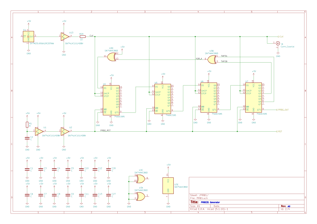
To build a PRBS31 generator, I will need a 32-bit shift register, which I’ll make by cascading four 74AHC595 8-bit shift registers. I will need to XOR the bits 31 and 28 and feed them to the data input. For that, I’m using the SN74AHC86 quad XOR gate IC. This serves to fully utilize the PRBS31 stream, and to get max possible bit stream length of 2,147,483,646 bits. At 25 Mbps, this will ensure cca 1.5 minutes of completely random bits. Now, the most obvious issue here is that, at first instance, when the all outputs are low, or undefined, the shift registers will stay in all-zero state. For this reason it is crucial to provide some initial, or seed value that ensures the gate will eventually change their state. I do this by XOR-ing feedback with “1”, that is effectively XNOR-ing the feedback. I am also using the double Schmitt-triggered inverter 74AHC1G14 to keep the outputs in the low state at the startup time.
Clock source and buffer
Now that the general architecture is defined, time to think of the clock source. It has to be relatively stable and reliable, but no crazy ppms are necessary. Standard crystals oscillator will do. The ready available one on LCSC is SX7M25.000A10F20TNN from the company called SCTF. Never heared of them. Hopefully, it’ll do the job. However, something that shouldn’t be relied on hope, but on a good engineering practice is the capacitive load this oscillator is facing. It clocks into 5 shift registers (4 in PRBS block, and one more in pre-emphasis block, more about that later). Each of them has two clock inputs. The input capacitance at each input is 3 pF but it can be as high as 10 pF. So, up to 100 pF in total. Hmm, how does this affect a stand-alone oscillator? Well, as the first, it can mess up its Barkhausen criteria. You know, the stuff that makes it oscillate. Second, it might not have enough of the drive strength to charge those 100 pF at the given rate. And indeed, the datasheet specifies the output load capacitance to be 15 pF.
That means that I’ll need the clock driver. The Schmitt trigger inverter 74AHC1G14 I used for the reset might do, so I’m just gonna put one in a call it a day. But let me just check some numbers real quick… I’ll need to charge this capacitance at the rate of 5V/5ns, since that’s the oscillator’s rise time. This converts to the peak current of
I_p = C\dot \frac{V_{CC}}{t_r} = 100 pF \dot \frac{5V}{5 ns} = 100 mA
Uh, oh. This is a bit too high. The absolute limit output clamping current of the 74AHC1G14 (and really other 74AHC family members) is 25 mA. Luckily, this is only the peak current, that bursts only during the level transitions. The average current would be
I_avg = C \dot V_{CC} \dot f = 100 pF \dot 5V \dot 25 MHz = 12.5 mA
This is a bit more comforting, but still, the output current at 5V supply is specified at 8 mA. So, this inverter might not be well suited to drive 25 MHz clock at this capacitive load. Let’s better find the the more suitable one. Quick browse through the vendor’s list delivers the SN74LVC1G14, from a bit more powerful family of 74LVC (low-voltage CMOS). Usually, this family works with 3.3V supply, but this particular chip can work with 5V as well. This chip has a max limit at 100 mA and delivers 32 mA normally. And while I’m at it, I might as well change my reset inverters to this type, a good practice to optimize the BoM.
For a good measure, I’m adding a series termination resistor. Not much, but it should prevent ringing, if there is any.
Decoupling capacitors
Just sprinkle 100nF ceramic caps all over the place and job is done!
Wait. Are we sure about that? Should we check the capacitors specs first? Here is for example very rich datasheet from Yageo, a well known MLCC manufacturer. Lets take a look at this interesting graph:
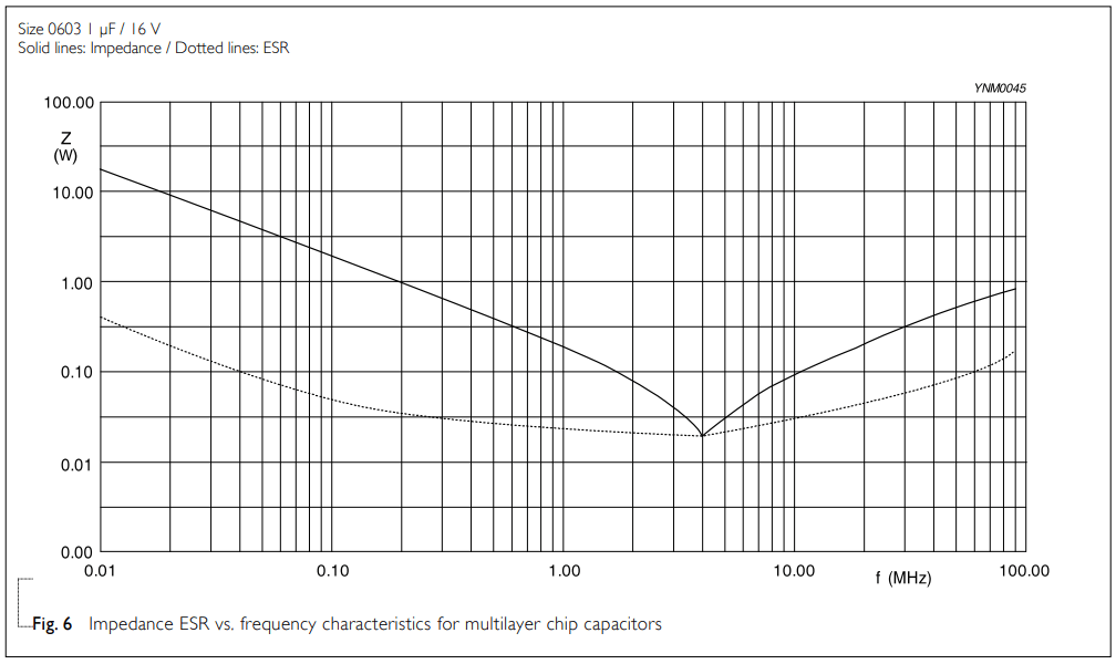
The impedance characteristics of a very common 1uF in an also very common 0603 package looks a little bit worrying – the cap reaches the self-resonance at cca 4 MHz, and at desired frequency range it already doesn’t behave like the capacitor! Just by scaling down the capacitance for order of magnitude, with the same ESL (which is of course defined by the package size), I can expect the resonance at 12.5 MHz for 100 nF in the same package. Should I go for more capacitors, or should I use the smaller sized ones and optimize for the least ESL?
Let’s break it down and start with transient current.
In my circuit, one shift register has one output that drives the input of another shift register. Earlier, I mentioned that the input capacitance is about 10 pF per input, and the rise time is 5ns. This translates to 10 mA of transient current that decoupling capacitor needs to supply.
Now the voltage.
Max allowed voltage droop is the value VCC can drop down during the transient without messing the logic states. For example, in case of 74AHC595, lower threshold for the logic HIGH is 3.94V for a supply of 4.5V. So the max allowed droop is 560 mV, right? Almost. The VCC droop is not the only factor that messes up logic states. There is noise, like crosstalk, ground bounce or simultaneous switching noise. Combined, they should never reach this lower barrier. So, lets plan for the 100 mV of max allowed droop, shall we?
Why would the VCC voltage drop down in the first place?
That 10 mA of transient current we estimated earlier? If it passes through the effective inductance of cca. 1 nH, what is a reasonable value to expect for the via in 1.6 mm PCB, then through the 1 nH of ESL in 0603 MLCC, and then through the lets say 1 nH of PCB traces more, for a good measure, what is going to happen? It will drop for L times dI/dt, or in other words, 6 mV. Way below the 100 mV we agreed upon earlier. So that’s good – 0603 cap shouldn’t be much of trouble here.
Now, how much capacitance do we actually need here?
The charge delivered by the decoupling capacitor is dynamic current of 10 mA times the rise time of 5 ns, what is 50 pC. Capacitor should deliver this charge during the transient without drooping more than 100 mV across. So, C = Q/U, or 0.5 nF. The 100 nF mentioned before should cover this more than enough.
As I said at the beginning of the section, just sprinkle 100 nF ceramic caps all over the place and job is done!
Here’s the first part of the transmitter, the PRBS generator circuit:
Manchester encoding
Funny enough, I came to encoding part of my design, only after I started thinking about the receiver side. I want to transmit a PRBS data stream over a channel and ensure the receiver can reliably recover the clock from the data itself. The problem with sending raw NRZ (Non-Return-to-Zero) PRBS data is that it can contain long sequences of identical bits (e.g., many consecutive ‘1’s or ‘0’s). Clock Data Recovery (CDR) circuits in receivers need frequent transitions (edges) in the data stream to stay synchronized with the incoming data rate. Long periods without transitions can cause the receiver’s clock recovery mechanism (like a PLL) to drift off frequency, losing lock.
To solve this, I’ll need to encode the raw PRBS data stream before transmission using a line code that guarantees a minimum density of transitions. Some common approaches are Manchester encoding, 8B/10B or 64B/66B. The latter two consist of mapping 8-bit or 64-bit long data and several control values into 10 or 66-bit long symbols. The 64B/66B was invented for purposes of 10 Gbps Ethernet, and is practically unachievable without FPGAs or dedicated ASICs. The 8B/10B got me thinking for a while, if I could do it with off-the-shelf discrete components. I could use EEPROM for look-up table storage, and some discrete logic to latch the input data, calculate the disparity of the output symbol, update and store the running disparity state for the next cycle’s lookup, synchronize the whole process… It would be immensely complex and out of the this project’s scope, but maybe, just maybe, I could try it.
The definite “No” got me when I started thinking about memory access. 10-bit long symbol at 25Mbps data rate would need a symbol clock of 31.25 MHz. New symbol should be available every 1/31.25 = 32 ns. The standard memory chips like AT28Cxx have memory read time in order of magnitude of 100 ns. This means that by the time the EEPROM could even retrieve the 10-bit symbol corresponding to one input byte, several new input bytes would have already arrived. It simply cannot operate fast enough to perform the lookup in real-time for each symbol. Maybe I could find some faster memory chips out there, but it would be too much overkill for the project like this.
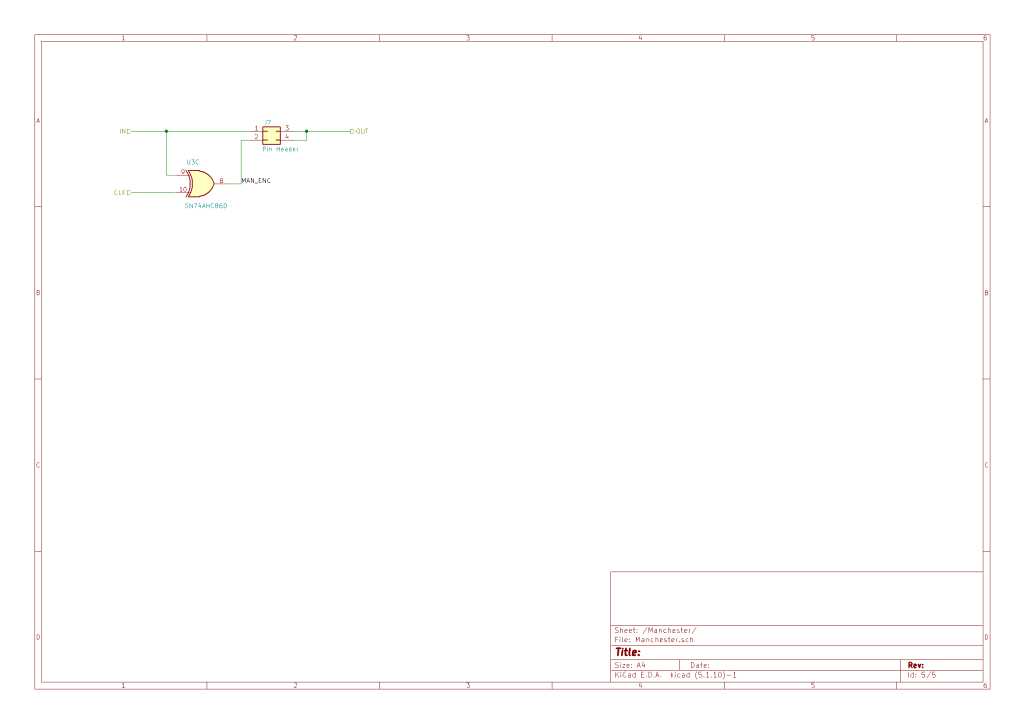
So I settled down for the Manchester encoding, the simplest way to do the encoding on the discrete component design like mine. Manchester guarantees enough transitions (at least one transition per clock cycle) and is DC balanced as well, another important feature for differential link transmission. There is a downside, nonetheless. Manchester doubles the required bandwidth. The logic family I’m using here, 74AHC is already stretched at 25 Mbps. I am not so sure if it could pull 50 Mbps off. However, I’m building it by XOR-ing PRBS data input with the clock. This is the most basic implementation of the Manchester. I am also leaving option to disable the encoding at all in case it doesn’t work or that I’ll have to use the slower clock.
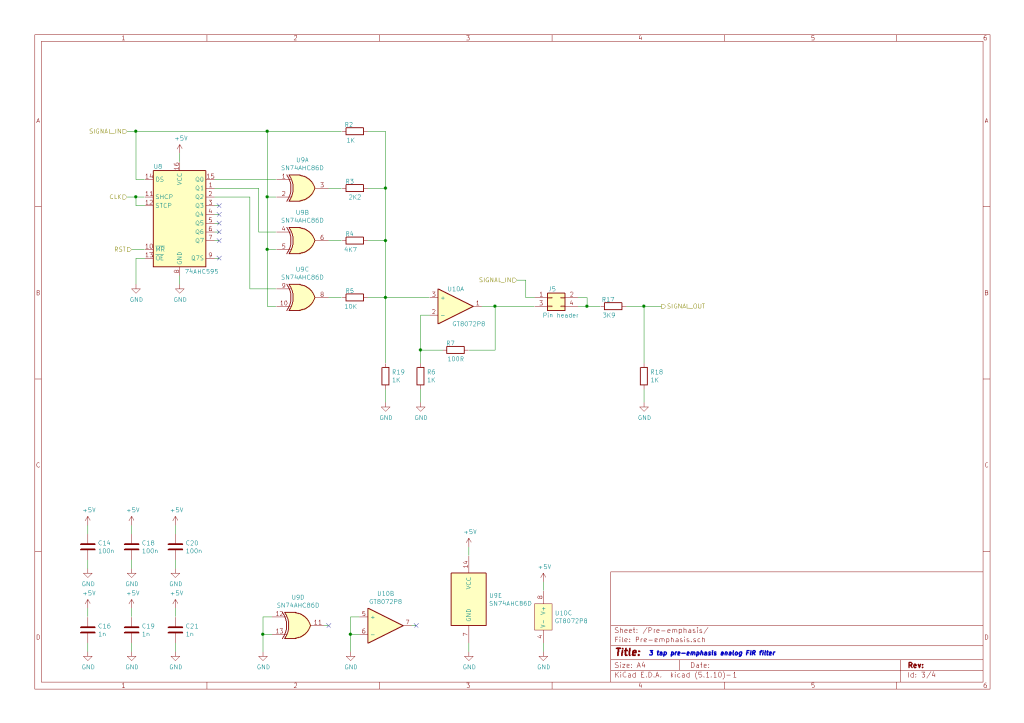
Pre-emphasis
Thinking about the pre-emphasis was what got me into this project. I’ve known for years that high-end transceivers use pre-emphasis to fight signal integrity degradation over the lossy channel, but I never knew how exactly they do that. I know there is some FIR filter involved and that some taps are used to increase the high-frequency content of the signal. This results in a pronounced spikes at the signal’s edges, that is, where bit transitions occur.
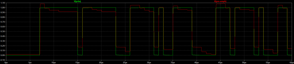
My implementation here is analog version of the FIR filter. I am using again a 74AHC595 shift register to reach out 3 taps of the FIR filter. Then, each tap is XOR-ed with the original signal – this way the transients are detected (XOR output is positive only if previous state was different than the current state). Finally, the XOR outputs scaled down and added to the original signal. I am using a classical op amp summation circuit that will add different weights of taps together. I am expecting a get something like this at the output:
To make this feasible, I will need the wide bandwidth op amp, that has at least 5x nominal frequency bandwidth size, as well as high slew-rate. I want to be as carefree as possible about damping the transmitter signal at this stage in the transmitter design. At the same time, I don’t want to pay much more than a couple of cents for it. So, let’s see what is available out there. I gave it some time to search through the stock, and listed some of the viable solutions down here:
| Slew rate & BW | Settling time | Price | but… | |
| COS8092 | Middle (200 V/µs & 300MHz) | 50 ns | $0.35 / piece | too tight for my design |
| GT8072 | High (420 V/µs & 500MHz) | Non specified | $0.27 / piece | A lot of info missing |
| TPH2502 | Middle (200 V/µs & 250MHz) | 25 ns | $0.85 / piece | not a big improvement |
| AD8039 | High (365 V/µs & 300 MHz) | 18 ns | $5.20 / piece | a tiny bit too expensive |
| AD8062 | High (650 V/µs & 320 MHz) | 35 ns | $4.55 / piece | still to expensive |
| AD8008 | High (650 V/µs & 740 MHz) | 18 ns | $4.36 / piece | looks the best, but still too expensive |
| OPA2830 | Middle ( 500 V/µs & 230 MHz) | 44 ns | $2.50 / piece | extra long settling time worries me |
| OPA2356 | High (300 V/µs & 450 MHz) | 30 ns | $3.30 / piece | I feel there are better options |
| LMH6628 | High (550 V/µs & 300 MHz) | 12 ns | $4.28 / piece | if only the price was a little bit… |
| LMH6658 | High (470 V/µs & 270 MHz) | 37 ns | $2.10 / piece | Might be the one! |
Browsing through this hasn’t been so easy. What I found is that op amps with high BW/ slew rate usually take more time to settle, with settling time ranging to 30 – 50 ns, easily. Also, the same amplifier has much different characteristics with the bipolar and the unipolar supply. For example, LMH6658 will have 700 V/µs when supplied with ±5 V, but only 470 V/µs when supplied with single 5V source. LMH6228 which has the best settling time supports unipolar supply, but specifications are only listed for bipolar; it might happen it performs worse when I power it with 5V alone. Maybe settling time doesn’t play a big role here – I am not doing any precision measurements, so oscillations of 0.1% are tolerable, I guess. On top of that, all the reliable pieces, that is, chips made by Texas or Analog, have a price range of 4 to 5 bucks. Asian brands do not boast with very high performance and I appreciate their honesty! There is one tiny chip that might just hit the right spot: GT8072. This is probably just a knock-off of some obsolete AD’s chip, but costs 27 cents and might be well suited for the job.
Here’s what I’m going to do: I’ll put the cheap GT8072 chip and order some LMH6658 on the side. In case the GT doesn’t do the job well, I will simply drop in replace it with the LMH guy. For this reason, I am going for the standard dual amp SOIC-8 package.
My pre-emphasis block is shown in the figure below. There is a shift register, XOR gate and the op amp summation circuit. Each tap is scaled with the different factor, and, although I chose the default ratios as 1:2.2:4.7:10, I will most likely have to experimentally figure out and adapt on my lab desk. Checking with Mr. Kirchhoff and doing some circuit analysis, I figure that my op amp output will result in the following tap sum formula
UOUT=0.36*UIN + 0.16*UTAP1 + 0.07*UTAP2 + 0.03*UTAP3With the 5V logic, the actual voltage levels are 1.8V for the base line and 0.8V, 0.35V and 0.15V for each of the taps, respectively. So, it is to be expected that, in case of single 0 to 1 transition, pre-emphasized signal peaks at around 3.1 V. This should keep the op-amp below the saturation limit. Slew-rate of around 400 V/us will make this slope within 8 ns. I guess good enough for my purpose here.
And finally, I’m planning for the possibility that none of the pre-emphasis theory actually works, and I can simply bridge the input all the way to the output. I am also adding the voltage divider of 0.2x, because I am expecting to change the output voltage level, as explained in the next section.
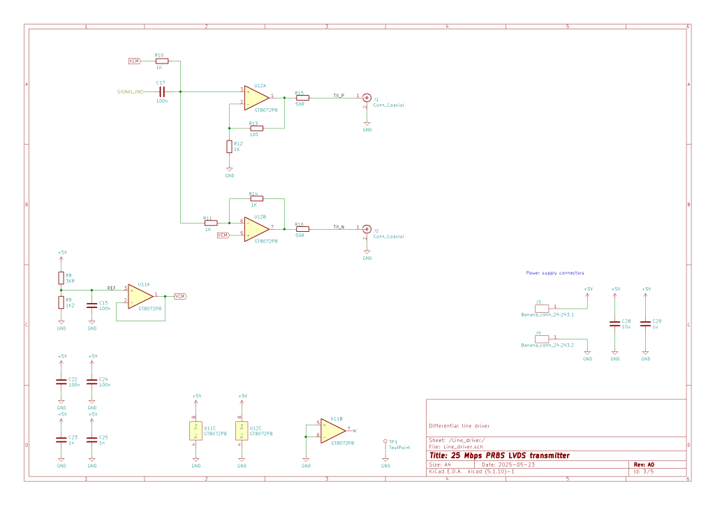
Line driver
The last step is to to make sure that the signal is ready to travel along the lossy 100-Ohm transmission line. I need to make it proper LVDS, that means: 1) changing the voltage level, 2) creating complementary pair, and 3) adding common mode. All of that while ensuring that outputs can drive 100 Ohm line. The LVDS standard assumes 1.2 V common mode voltage, 350 mV differential voltage swing, and capability of sourcing 3.5 mA output current.
My approach has two op-amp circuits, one inverting and one non-inverting. To make this work, I need to redefine the common mode voltage to 1.2 V. I do this by DC blocking the input signal and adding 1.2 V from the buffer as a new common mode point. Since my baseline signal after the pre-emphasis is 1.8V, the divider mentioned in the previous section will scale it down to 0.36 V, what is exact differential swing I am aiming for here. That’s why I’m using unity gain in both of my op-amp circuits here. The op amps I intend to use will be the same type I had in pre-emphasis circuit, since the bandwidth and slew rate requirements are the same. The only additional requirement is the capability of sourcing 3.5 mA current, what GT8072 can easily do.
Finally, two outputs will have 50 Ohm output resistance and routed as a differential pair, terminated with the classic SMA connector.
Layout
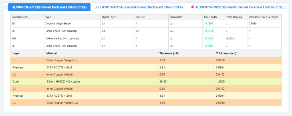
I decided to go with the JLC-PCB 4-layer stackup. Impedance needs to be controlled, and that’s why I originally chose stackup with 3313 prepreg. Their website does the impedance calculation for you and gives the trace width values for my controlled impedance traces. However, only after my layout was done, did I learn that 3313-based stackup design comes with the “standard” assembly price, instead of “economic” price, what brings the minimum amount of assembled boards to 5. This, of course, triples my planned costs. To avoid it, I had to revert to the default, 7628-based stackup, where the controlled impedance requires somewhat wider traces. Imagine my delight when I realized I’d need to redo the layout for this.
I put my high speed signals ( high speed 25 Mbps, LOL) on the layer 3, with the specific reason to reduce the via stubs. That way, reference planes will be on layer 2 and the bottom. Layer 2 is poured in copper and serves as a 5V plane, meaning that bottom is dedicated to the GND.
You might laugh off the notion of 25 Mbps as a high-speed stuff, but let’s be cautios for a minute here. First, there are harmonics, what makes the highest usable frequency on my board to cca 125 MHz (5th harmonic). Second, there is signal rise-time of 5 ns, which corresponds to the bandwidth a bit shy of 200 MHz. At that frequency, the quarter wavelength is around 20 cm. This is quite on the same scale as my circuit board. Some signals, like clock for example stretch easily to this distance (keep in mind, the clock signal has to reach five shift registers and one XOR gate, all in in SOIC packages). There will be also some stubs. I am pretty convinced we would see some transmission line effects, like ringing and reflection if the layout was done with no thought at all.
I ordered my PCBs and assembly services from JLC-PCB, opting to source the components directly from LCSC. It cost me around 70 bucks for PCB production, components sourcing, assembly and shipping. As I wait on my batch to arrive, I am onto the receiver design.
