Introduction
Being a freelancer, one can never stop improving himself, get a new trade or sometimes even to revise the things he has already mastered. With this in mind, I came across Advanced PCB Layout Course by Fedevel Academy, a hardware design/consultancy company by great engineer Robert Feranec. This post is about my impressions, experiences and some things that I learned during this course.
Why this course?
I’ve been using Altium Designer ever since my student days and I’ve considered myself a bit more than a decent user. I’ve designed multilayered boards with plenty of BGA components, MPUs with DDR3 interfaces, LVDS routing and all other, shall we say, advanced circuit segments. I’ve been working with the stuff you don’t find in less capable EDA tools like Eagle or Kicad, stuff like database libraries, internal version control, variants, IBIS models and Spice simulations. However, I still didn’t feel like I have everything under control and wasn’t comfortable enough to do any complex design, like a System-on-Board all by myself
First time I’ve heard about this course was on the Amp Hour podcast and Robert seemed like a nice guy. I’ve checked his website and past projects, and it was all truly impressive. The guy’s been building PC motherboards all by himself for decades now! On his course website, Fedevel Academy, he’s providing online courses in PCB design and I got immediately curious about the Advanced PCB Layout Course.
The course is not for free, it costs cca 200 bucks, but I had a gut feeling that I need it. You know that feeling when you go shopping for groceries and you end up buying cowboy boots in a motorbike store? Yeah, that feeling. Also, the advertisement “You will be practicing on a real high-speed board with 1.2GHz CPU and DDR3, PCIE, SATA, HDMI, LVDS, 1Gb Ethernet and more” was very appealing. Getting my hands on some real computer source files and a comprehensive guide through seemed worth the money.
![imx6_rex_module_top_HR[1]](https://helentronica.com/wp-content/uploads/2017/04/imx6_rex_module_top_hr1.jpg?w=300&h=174)
For the sake of this course, Robert and his company have developed computer based on a very powerful processor i.MX6 by Freescale (NXP) and 1 GB of DDR3 SDRAM. The computer consists of an MPU module (containing CPU, DDR3 and Ethernet chips and power supply), inserted on a computer baseboard that hosts all I/O connections. This amazing baseboard allows access to all kinds of ports: high-speed Ethernet, HDMI, LVDS, SATA, PCIE, micro SD, RS232, a couple of USB and audio ports etc. The best part – all of the design files are open source, and supporting this OSH community was the final reason I needed to go on a take the course.

The course outlines
1. Placement
It wasn’t clear to me from the beginning, but the course actually guides you through the complete layout process – from the scratch. In Lesson 1 you start with a simple classic component placement and Robert introduces you to some basic rules: put big components first, leave some room between MPU and DDRs, put the high current components as far as the other side of observable Universe and so on. This should give some insight on probable board final size. Take some time to think how to optimize it – the board space is a valuable resource.

When all of the big components, both chips and connectors, are placed you should go on a place decoupling capacitors underneath the BGA chips. Now, this is very iterative and annoying process, but Robert guides you through with really helpful fanout and positioning tips so you can make your capacitors nicely packed and not disturbing other signals in the future.
Second thing to take care of are the termination resistors. They make all the high-speed signal magic work and should be as close as possible to the main component. Contrary, the EMI filters and ESD protection that should be as far as possible from the component and close to the connectors.
At this point in time, you should have 3D models ready so you can immediately see which component will be a troublemaker in assembly process and plan accordingly. How to get the 3D models in your project? I usually have a couple of options: first one is Altium’s inherent footprint wizard, which gives you proper footprint for some standard package types, like QFN or SOT (in PCB library workspace go to the Tools → IPC Compliant Footprint Wizard and it will guide you nicely). If Altium turned out to be helpless, I usually look for open databases on Internet like GrabCAD. Only when I’m truly desperate, I go to SketchUp/SolidWorks and do my own modeling.

2. Layers and vias
Component placement is just to get our feet wet, and to do it only two layers are enough. However, to choose how many layers your PCB might need is really a science for itself. Usually, it comes down as a quality vs. cost issue. For instance, cheaper 4 or 6 layer PCB will be permeated with via stubs and poorly routed traces, while the more expensive 10 or 12 layer boards will have nicely shielded high-speed signals and separated power planes.
Speaking of high-speed signals, they are usually determining the number of layers. If you want the highest possible signal integrity (and you do) make sure that all signals that work with high-speed black magic are routed in a stripline fashion having uninterrupted ground planes above and below the trace. For instance, take the MS Paint masterpiece below: when the components are on the same side, there should be track routed on the blue layer in sandwich between brown and green ground planes. Also there should be a two microvia pairs (orange) to lower the track from the pad on top layer through two layers and bring the track back to top again.
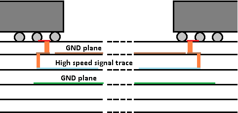
In case the components are on opposite sides, there should also be some buried vias that will lead the signal through all those ground/power planes in the middle from the blue to the purple layer. This way, we have avoided any open end via stubs that are true devils in high-speed signaling world. But keep in mind that the signal on upper side is referenced to the one ground plane, and signal on the lower side to the other. You should do a proper via stitching between all used ground plane. It is worth mentioning that one GND plane can be replaced with a power plane (as long as it’s uninterrupted), but in that case we have to make sure there is enough decoupling capacitors connecting these two planes.

Generally, when the board is complex as this one (i.e. any MPU board), top and bottom layers are reserved for really short tracks whether they’re fanout lines, inter-component connections or power traces. “Real” high-speed signal tracks are packed deep below the surface. Ground and power layers are usually stacked in the middle layers. GND and power planes in the middle may be broken and split into different power polygons, but those around high-speed signals should always be continuous and uninterrupted.
For iMX6 Rex module there are 12 layers foreseen with 4 microvia drill pairs, 1 buried via pair and, of course, 1 through hole via pair. These are the primary parameters that determine the cost of the board. Professional manufacturers will always take number of vias into account when quoting you a price.
3. Rules
Before doing any track drawing, one should always define rules for every specific net class that needs it. For instance, high-speed signals must have controlled impedance (most often 50 Ω for single ended signals and 100 Ω for differential pairs), and this is determined with the geometry of the trace. Therefore, we need a rule that sets the track width. Power tracks usually have to be as wide as possible.
There are tools available to help us determine those rules (even Altium has some kind of impedance calculator tool), but the best tool we get are our friends in manufacturing factories. Talk to them in regard of PCB stackup: how the boards are made, which materials are used for prepregs and cores and what are the thicknesses of copper and FR4 sheets. Knowing these values, you can define your stackup and use factory recommendations to define track widths, spacing etc. In iMX6 Rex case, they were cool enough to provide measures for every track type.

High-speed signal tracks are determined by the RF physics, while the power traces and vias are determined by thermodynamics. If components draw too much current, the poor via might burn out. And nobody wants that. So, calculate max. expected current of the system and plan the vias and power tracks accordingly.
A couple of rules that were new to me were 20H rule for power planes and 10x via ratio. The power plane should be retracted inside the board 20 x layer thickness millimeters more than other layers. Reason for this is reduced field scattering and there is a study there to back the rule up. Regarding via rule, the aspect ratio of the via should not be higher than 10 (via length/via diameter) in order to make via stable during the board production.
4. Fanout
Fanout was the thing I’ve never felt comfortable around. Doing some BGA soldering on my own, I knew the pitfalls of BGA soldering and wasn’t really confident about all those 0.1 mm vias around 0.5 mm spaced balls.
When starting the fanout, the best first step would be adjusting the grid to the BGA ball spacing. Altium has a nice feature, called Grid manager that enables you to create a grid in the constrained space only and you can use it for via placement in the middle among four ball pads.
First thing to fanout are power pins of MPU, and these usually require 0.3 mm through hole vias to connect them with the decoupling capacitor at the bottom side. Robert recommends to use one and only one via per each power pad. Don’t share a power via among the tracks of the same net!
Second, fanout the data signals. Use 0.1 mm microvia or whatever is your manufacturer’s minimum to bring the data signal down to the layer dedicated for high signals. Now, this part is very tricky – there is a lot (A LOT) of the data signals and this is a perfect way to get a nervous breakdown. Routing them for hours only to realize in the end that some of them you missed to take out, and you must delete hours of your painstaking work. So, I learned on the hard way always to slowly and carefully take every single pin from the inside out and prepare fresh pack of sedatives. A couple of tips I’ve picked up about the fanout:
- Of all data signals, DDR interface is the most critical one. Make sure it’s the first and the shortest one you’ll fanout.
- Always start fanout with the inner pads – they have the least space and it will be painful to break them out later.
- On DDR SDRAM chip side, make sure that data signals are fanout outside and address pins inside of the chip.
- Use the same topology for the signals of the same group – you don’t want those signals to propagate differently.
- For future reference, fanout all BGA pads. If there are some modifications in the future it will be painful to add new tracks.
One thing about fanout, and the whole layout process in general – you have to think ahead all the time. While doing the fanout some general idea about how to route your traces should exist, and some layout topologies known. Only then you can plan the fanout that will cause the least headache later. Robert is full of tips and tricks to make this process less troublesome I am grateful to him for sharing them.

5. Routing
Routing is always a headache and you can imagine what mess is going to be when you get to route a couple of hundreds of nets on a 3 inches board. Routing process should always start with a following step: reading manufacturer’s layout guidelines. For instance, NXP (and many others) recommends to route DDR3 interface first, but in following order: address signals, differential pairs, control signals and, finally, data signals.
A couple of the most useful thing I’ve learned about routing:
- Route piece by piece. Never route one signal at the time from beginning to an end, followed by the other signal the same way. Always start with all signals from the group and route them bit after bit.
- Route from both ends at the same time. Carefully route the signals around the obstacles and make two ends meet somewhere in the middle.
- First, do it rough, and refine it later. Refine it in many iterations. Make sure signals from one group are all interconnected first, and tweak them later.
- Signals of the same groups (i.e. DDR data banks) always route the same way. So, the same number of vias for every signal, the same layers, the same curvature etc.
- Set different color for different signal groups! I’ve seen many professional designers never doing this – probably finding coloring something as a childplay, but in this situation it’s a lifesaver. And it also makes PCB look hippie.
In DDR3 interface, address and control signals are shared among all memory chips, so, the best way to route them is T-branch or Fly-by topology. On the other side, data banks are dedicated per each chip and should be routed in separate groups. Routing data signals usually gets easier with the pin swapping but one should always be careful not to swap the unswappable pins.


Length matching
Once the data signals are routed, comes the real problem – the length matching. If we don’t want throw the PCB in the garbage after long, assiduous routing, proper length match is “a must”. It is the best to do the preliminary length matching immediately after the routing:
- select all the nets from the same group (make Net Class a priori),
- sort the nets by length
- manually shorten the longest net as far as it goes
- extend all the remaining nets from the group to match the longest one as close as possible.
Keep in mind, this is a preliminary length match only. It is highly recommended to do it manually at the beginning of the layout design. Later on, at the end of the design, Altium offers a handy length matching tool to tweak the traces in more precise way (Tools→Interactive Length Tuning). For high-speed signal, like PCI Express, it is necessary that tracks are the same length on all layers. Make sure that the same signal portions on each layer are equally long and always route all signals of the same group in the same way. Also, keep in mind that signals at the surface layers travel at the different speed than the signals within the board. Engineers at Intel or AMD take all of this into the account. They create special spreadsheets to calculate signal lengths on all layers separately, including vias, termination resistors, pins and even length mismatch on the silicon die.


Speaking of length matching, one situation where it is of crucial importance are differential pairs. Not only do these guys need to be routed exactly at the same length, we must ensure that the signal edges at + and – tracks are traveling together So, for instance, when one pad is a bit behind that its pair, you should compensate the difference with a meander patterns immediately after the fanout. This is the only way that + and – edge of diff. pair are traveling along each other.

Crosstalk
Crosstalk is the thing that came straight from hell. It’s an eternal nemesis of digital PCB designers. Typical rising time for CMOS signals is less than 10 ns, enough to cause decent crosstalk. For example, on two layered 1.6 mm PCB, 8 cm coupled signal length is enough to cause 3V crosstalk. (use PCB calculator if you don’t believe). The spacing will not reduce it significantly, nor will the length of the traces. Only thing that can reduce it is a thinner PCB. Use multi-layered 0.1 mm PCB for high-speed boards.
Rules for the crosstalk include proper spacing of the signals and keeping different groups away from each other. If the H denotes the height of the PCB, there are some practical rules for spacing values:
- for Clock & Data signals: 7H at the surface and 5H inside the PCB
- for ADDR & CTRL: 5H at the surface and 3H inside the PCB
Altium is very helpful when it comes to the crosstalk simulations and other signal integrity issues. Make sure to check the possibility of the crosstalk simulation to be on the safe side.
6. Release
When you think you’re finished with the routing and finally the design process is over, you’re 50% done! Now, it’s time to review everything, slowly and carefully. Take your time, clear your head, and come back to your design a day or two later. There can be no way to emphasize this enough: check everything carefully. If I have to take only one thing from this course, it would be this rule: check everything carefully. There is always some track to be shifted or length-matched, or some via put on the wrong place. So, check everything carefully. Then, relax and let the DRC tools do their thing.
At the end of the course, Robert gives practical advice on releasing production and assembly data in professional way. Working in the industry, I was already familiar with those concepts but let’s put them here for the sake of rounding up the post. If you’re designing something like computer motherboard, chances are, you’re not going to make the PCB in you home lab with CuCl2 bath and solder iron. You’re going to make a professional manufacturer do it. The data he cares most about is the artwork of your PCB, drill drawing, assembly drawing, bill of materials, pick and place file and eventually 3D model. It doesn’t seem like that, but it is a lot of files and you get into the mess easily. Especially if the project and company require specific filename standards. Managing those files is something Altium does really well, using its Output Job files and Release Manager. Setting up the output job files and clicking one single button solves the release issues in no time and your PCB is ready for the production.
Conclusion
I’ve been comfortable with microwave and high frequency circuit boards for a long time now. For those kinds of challenges, there were always more or less straight forward rules: a lot of ground area, lots of vias, and keep everything short, tidy and far away from the other components. High-speed signal design is very similar, but not quite alike. High-speed signal design is microwave design but with many more frequencies at the same time, and many more routes that must be packed in tiny area. There is no comfort in plenty of room that microwave filter or amplifier provides. In other words, there’s a million ways things can go wrong and your months-long work into the garbage bin.
PCB layout is a form of art in its way, except when it is painstaking, iterative, monotonous and nerve-breaking. You can get easily discouraged when you’re facing 24-layered board, thousands of nets and requirement to route them in a couple of inches board. Are the traces too long, are the too close, is the impedance matched, is the current too high, are components heating each other too much, are questions you’ll have to answer for each track you’re routing. A system complex as a computer motherboard or, as in this case, a single-board-computer, consists of many complementary things – power components and switching noises next to the crosstalk sensitive SDRAM tracks, fast rising times and 20 cm long tracks of HDMI interface, etc. Your brain works like the steam locomotive when you’re designing it and you’re afraid all the time that you’re doing something wrong.


However, there is a way to confront those questions. I found it while working on the projects from this course, having the chance to design the whole iMX Rex by myself. It is the guided practical experience and extensive theory backup that made me understand high-speed and high density circuits clear and understandable. Robert’s course has made me feel confident with designing extremely complex circuit boards completely on my own. It has given me a set of tools and know-how skills to tackle high-speed circuits like GPU and CPU motherboards and their integration with computer peripherals. With that in mind, to the new projects!

2 thoughts on “Advanced PCB Layout Course by Fedevel Academy”