Introduction
Having my reflow solder oven finished, I couldn’t wait to see how far can I challenge it with complex circuit boards and tiny components. I decided to build a system with components that are tricky to solder, such as BGA and QFN packages. Not interested in designing the whole circuit on my own, I looked for an existing solution and found a good-looking one: an embedded Linux computer by Henrik Forsten.
The circuit
To build a bare minimum Linux computer, one needs a decent processor and some memory. It won’t be a very useful computer, but it’ll run Linux kernel, some processes and you’ll be able to open a bash terminal on it.

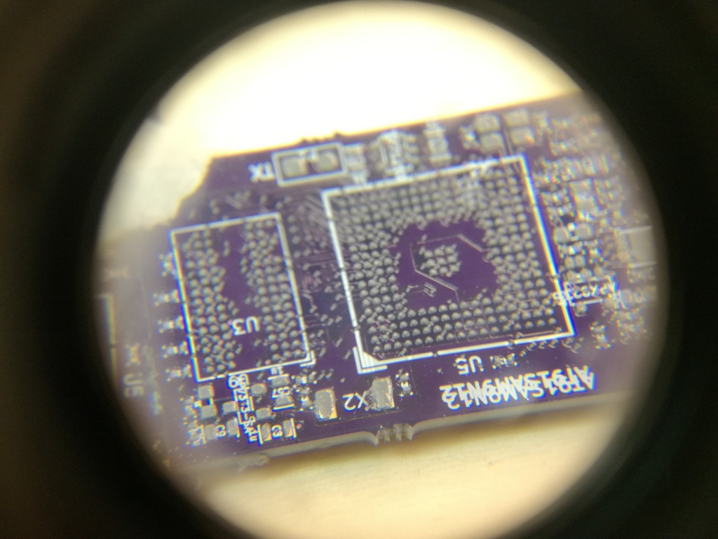
By decent processor I mean a microprocessor with a Memory management unit (MMU) and by memory I mean some RAM (for OS to work, obviously) and some Flash (for OS to boot, more obviously). Henrik decided to base his design on an Atmel’s 32-bit ARM9 core AT91SAM9N12 microprocessor. Now a bit outdated, but still very powerful chip that will serve well the educational purpose of this project. The processor is packed within the disgustingly small LFBGA package with 217 tiny balls spaced by 0.8 mm and 0.5 mm in diameter each. This is a challenge not only for home soldering equipment but also for a manufacturer: you need to keep in mind that both vias and tracks on the pcb will be significantly small and not many pcb producers will be able to do it. More details on fabrication issues Henrik has written on his blog.
 Accompanying processor there is 64 MB DDR2 SDRAM chip W9751G6KB that will serve as a working memory (colloquially called RAM). The memory comes in 84-TFBGA package with also 0.8mm spaced balls, just in case that processor is not annoying enough.
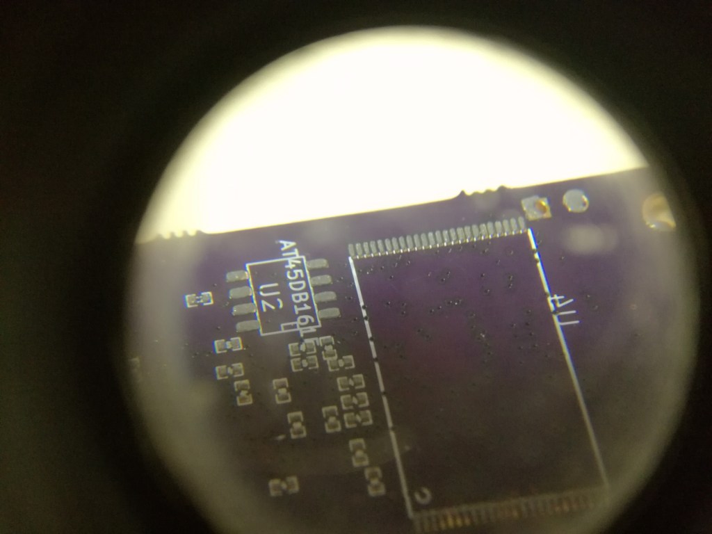
 As a mass storage memory 4 Gbit (or 512 MB) NAND memory S34ML04G2 was chosen. Slightly more comforting as it comes in 48-TFSOP package, that has 0.5 mm pin spacing. It would still be a decent mess if you do it by hand and don’t have a lot of practice in your hands. Btw, in case you are a bit confused with these memory acronyms, here’s my last post where I tried to clarify various memory types.
Aside from the main components, processor and memories on a circuit board there are voltage regulators for 3.3V, 1.8V and 1V as well as a reset controller chip. These components are regular SOT packages except 3.3V regulator that is PAM2321 chip in WFDFN package (that is just like QFN but without “quadratic”). There are also two USB connectors on board: one micro USB type B for device functionality and one type A jack for a host functionality, that will be used for installing Linux image from a USB stick. Passive components like capacitors and resistors were all taken in 0402 package mostly (a couple of them came in 0603) to make production a bit more tricky.
Circuit schematics, pcb layout as well as all software is available to check in on the Henrik’s Github repo.
Building the hardware
Like Henrik, I’ve also ordered my pcbs from OSH Park, stencils from OSH Stencils and components from Digi-Key. The building process is:
- cleaning the board (and your throat) with some alcohol.
- applying a bit of a liquid flux to remove the corrosion
- applying solder paste
- making mess everywhere I can with the solder paste
- ruining my clothes, table, hands and face with the solder paste
- pick’n’placing the components on the solder paste artwork you’ve just made
- baking everything in the reflow oven as delicious Christmas cookies. And just like in the Christmas time, you hope for the miracle next minute you take your pcbs out of the oven.
- turn the board upside down and repeat all the steps since there are two sides to go. In this case all components on the bottom side are lightweight so the surface tension will keep them attached to the board while you solder top side.
- Enjoy the fun of electronics assembling!
BGAs, QFNs, TSOPs and 0402s – everything for a nice little soldering challenge. What could go wrong?


But does it work?
Soldering finished and hardest part done! Everything looks nice, but we’re still far away from the finished product. Are all pins placed properly? Are there cold junctions? Shorts? Open circuits? Apart from optical inspection not much can be done to determine mistakes – BGAs have the tendency of not showing their, hmm, balls to the world and we can’t se if the component has been properly soldered. The only thing we can do now is to plug the board and hope for the best.
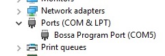 Atmel pre-loads their ARM chips with a boot loader that appears as a virtual serial device on your computer. If everything worked well, after connecting it to your PC there should be a “bling” sound coming out and a “new device connected” message. That means that the processor is well-connected and working.
Atmel also distributes a program called SAM-BA that is a boot assistant for SAM chips (get the name, SAM-BA) that is used for programming, debugging and just casually walking through the AT91’s memory space. Opening this program should guide you to connect to the virtual serial port and the device you’re using, that is, AT91SAM9N12 board.
SAM-BA also allows execution of scripts (which you need to learn to write) that let you do more advanced stuff. For instance writing and reading the external memories. This is a way to verify that your memory chips are also nicely connected.

As can be seen from the screenshots above, everything worked. This came as a shocking surprise! Is it possible, in engineering world, that something works from the first try?

Very nice indeed, amazing !!!
May be stupid question how do you reflow both side? Top and bottom ?
Not a stupid queston: first I reflow bottom side where there are less components (and lighweight ones). When it’s done, I take it out, turn upside down, put the paste on the top side, place the components and reflow again. Now, the bottom side component are upside down, but the surface tension of the solder keeps them from falling off the board. They are really small 0402 packages so the surface tension can overcome the gravity 🙂
Isn’t the melting point of the solder paste higher once it has become solid, and thus it will not reflow at the same temperature as the solder paste?
“Is it possible, in engineering world, that something works from the first try?”
Nope 😉
“Is it possible, in engineering world, that something works from the first try?”
No, if works on the first try, means that the bug is still hidden. 😀
Can’t see most of the images
Thanks for the feedback. I think it is fixed now, isn’t it?
I can see them all fine.
Thanks for awesome inspirational post. It inspired me to try!.. I’m still busy with the schematic but I am confused already… I see a bus with a DDR_A global label.. and a label of SDA10.. but when I look for SDA10 elsewhere I only see it on the EBI_A bus. Is it possible for one bus (EBA) to connect to another (DDR_A) just for that one wire?